Field emission display with reflection layer

a field emission display and reflection layer technology, applied in the direction of discharge tube luminescnet screens, discharge tube main electrodes, discharge tube/lamp details, etc., can solve the problems of low efficiency of the phosphors layer, contamination of the display panel is not easily prevented, and the manufacturing process is very complex, so as to reduce the phosphors layer efficiency and raise the lighting efficiency. , the effect of low efficiency

Inactive Publication Date: 2005-09-08
TECO NANOTECH CO LTD
View PDF4 Cites 5 Cited by
  • Summary
  • Abstract
  • Description
  • Claims
  • Application Information

AI Technical Summary

Benefits of technology

[0011] The prior art uses a low actuating power voltage of less than 5 KV. This is the major reason for the low efficiency of the phosphors layer. The conventional technical uses the reflection layer to raise the lighting efficiency, but the manufacturing process is very complex. In addition, in another conventional technique, contamination of the display panel is not easily prevented. The present invention thus provides a new insulating supporting device 38 with the reflection layer to raise the lighting efficiency of an FED. The installation process of the insulating device of the present invention is very easy. The insulating device of the present invention is also easy to manufacture independently with a low failure rate in quality.

Problems solved by technology

This is the major reason for the low efficiency of the phosphors layer.
The conventional technical uses the reflection layer to raise the lighting efficiency, but the manufacturing process is very complex.
In addition, in another conventional technique, contamination of the display panel is not easily prevented.

Method used


Image

  • Field emission display with reflection layer
  • Field emission display with reflection layer
  • Field emission display with reflection layer

Examples


Embodiment Construction

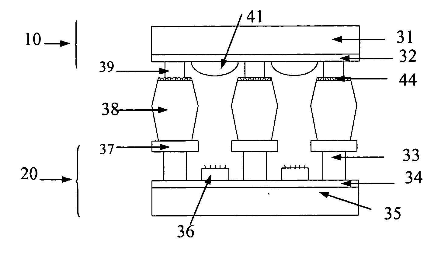
[0026] The present invention provides an insulation supporting device 38 with a reflection layer. Reference is made FIG. 5, in which the insulation supporting device 38 is made of an insulating material with a thermal expansion modulus similar to that of the anode structure (plate shape) or the cathode structure (plate shape). The said similar thermal expansion property can be useful when the heating process is applied to the FED panel, avoiding an expansion difference that would crack the FED panel surface. The said insulation supporting device 38 has a plurality of holes 42 that is arranged according to the cells of the anode structure or the cathode structure. The holes can act as the tunnels for the electrons from the cathode to pass through to strike the anode. The holes are formed by, for example, etching. For the special feature of the invention, a reflection layer 44 is installed on one side of the insulation supporting device 38. Reference is also made to FIG. 4 to illustra...


PUM


Abstract

A field emission display with reflection layer has an improved insulating supporting device. The major feature is to place a reflection layer on the insulating supporting device. From the special structure, the insulating supporting device can enhance the emission efficiency of the phosphors powder rather than the primary function of the insulating support. The field emission display with reflection layer has an anode structure, a cathode structure and the supporting device.

Description

FIELD OF THE INVENTION [0001] The present invention relates to the structure of a field emission display. The feature is related to the reflection layer settled on the insulating supporting device between the cathode and the anode with a special effect of raising the brightness of the field emission display. BACKGROUND OF THE INVENTION [0002] There are various kinds of flat panel display (FPD) including, for example, field emission display (FED), liquid crystal display (LCD), plasma display panel (PDP), organic light emitter device (OLED), and liquid crystal projection display. The common features of such displays are that they are thin and light weight. According to the property of every flat panel display, some of them can be applied on the small scale panel for devices such as cellular phones; only a few are suitable for application in medium or large scale devices such as computer monitors or TV displays. Yet another application for flat panel displays further comprises super la...

Claims


Application Information

Patent Timeline
Patent Type & Authority Applications(United States)
IPC IPC(8): H01J1/62H01J19/24H01J61/38H01J63/04
CPCH01J29/862H01J2329/89H01J31/127H01J29/89
Inventor HSIAO, CHI HUNGFANG, JIN-SHOUCHENG, KUEI-WEN
Owner TECO NANOTECH CO LTD
Why Eureka
Try Eureka