ESD protective circuit with collector-current-controlled triggering for a monolithically integrated circuit

a monolithic integrated circuit and collector current technology, applied in the direction of emergency protective circuit arrangement, transistor, etc., can solve the problems of leakage current via the trigger circuit, clamp triggering, gate oxide or diffusion layer damage of i/o transistors, etc., to avoid leakage current or inadvertent triggering, and prevent damage to the circuit to be protected.

Active Publication Date: 2005-09-08
INFINEON TECH AG
View PDF6 Cites 49 Cited by
  • Summary
  • Abstract
  • Description
  • Claims
  • Application Information

AI Technical Summary

Benefits of technology

[0014] An ESD protective circuit is provided which offers even more reliable protection against ESD loads. In particular, in the event of an ESD load at an input or output of a monolithically integrated circuit, a low-impedance ESD discharge path is provided as early as possible, that is to say even while the magnitude of the potential of the input or output is low, so as to reliably prevent damage to the circuit to be protected. Leakage currents or inadvertent triggering are also avoided.

Problems solved by technology

In the process, the gate oxide or diffusion layers of the I / O transistors is or are generally severally damaged or even destroyed.
Setting the trigger threshold to a low level such as this has the disadvantage that, when the integrated circuit is being operated at high temperatures, this can result in leakage currents via the trigger circuit and possibly also flowing via the power clamp, or the possibility of the power clamp being triggered inadvertently.
In both situations, the functionality of the integrated circuit can be massively adversely affected: leakage currents cause an additional power loss, while inadvertent triggering results in a short circuit between the supply networks and can be rectified only with difficulty during operation of the circuit.
The base potential change associated with this results in a drain-bulk breakdown of the LVTSCR-inherent MOS transistor.
This drain-bulk breakdown results in triggering of the respective thyristor.
This solution has the disadvantage that the triggering of the respective thyristor via the drain-bulk breakdown of an MOS transistor does not occur until the potential at the I / O pad has a specific magnitude, even if the magnitude of the potential is reduced further after the triggering.
If the potential magnitude before triggering of the thyristor is also only briefly above the critical magnitude mentioned above, damage to or destruction of the circuit which is connected to the I / O pad internally cannot be precluded despite the presence of an ESD protective circuit.
The risk of ESD damage is in this case particularly high with modern semiconductor process techniques with structure sizes in the sub-0.1 micrometer range.
The diodes are connected such that they do not provide a conductive connection during normal operation of the integrated circuit.

Method used


Image

  • ESD protective circuit with collector-current-controlled triggering for a monolithically integrated circuit
  • ESD protective circuit with collector-current-controlled triggering for a monolithically integrated circuit
  • ESD protective circuit with collector-current-controlled triggering for a monolithically integrated circuit

Examples


Embodiment Construction

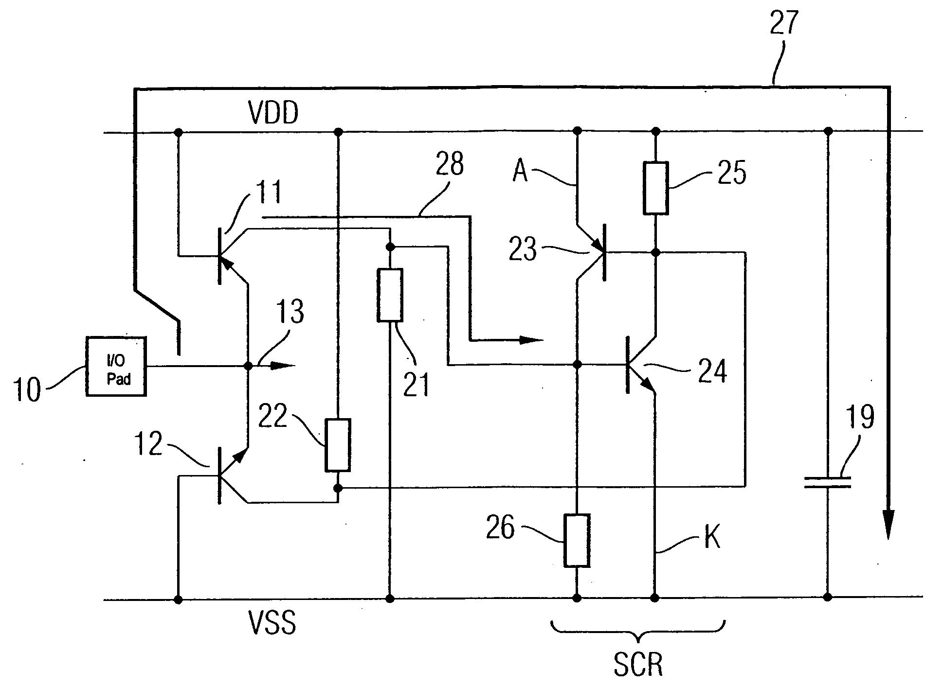
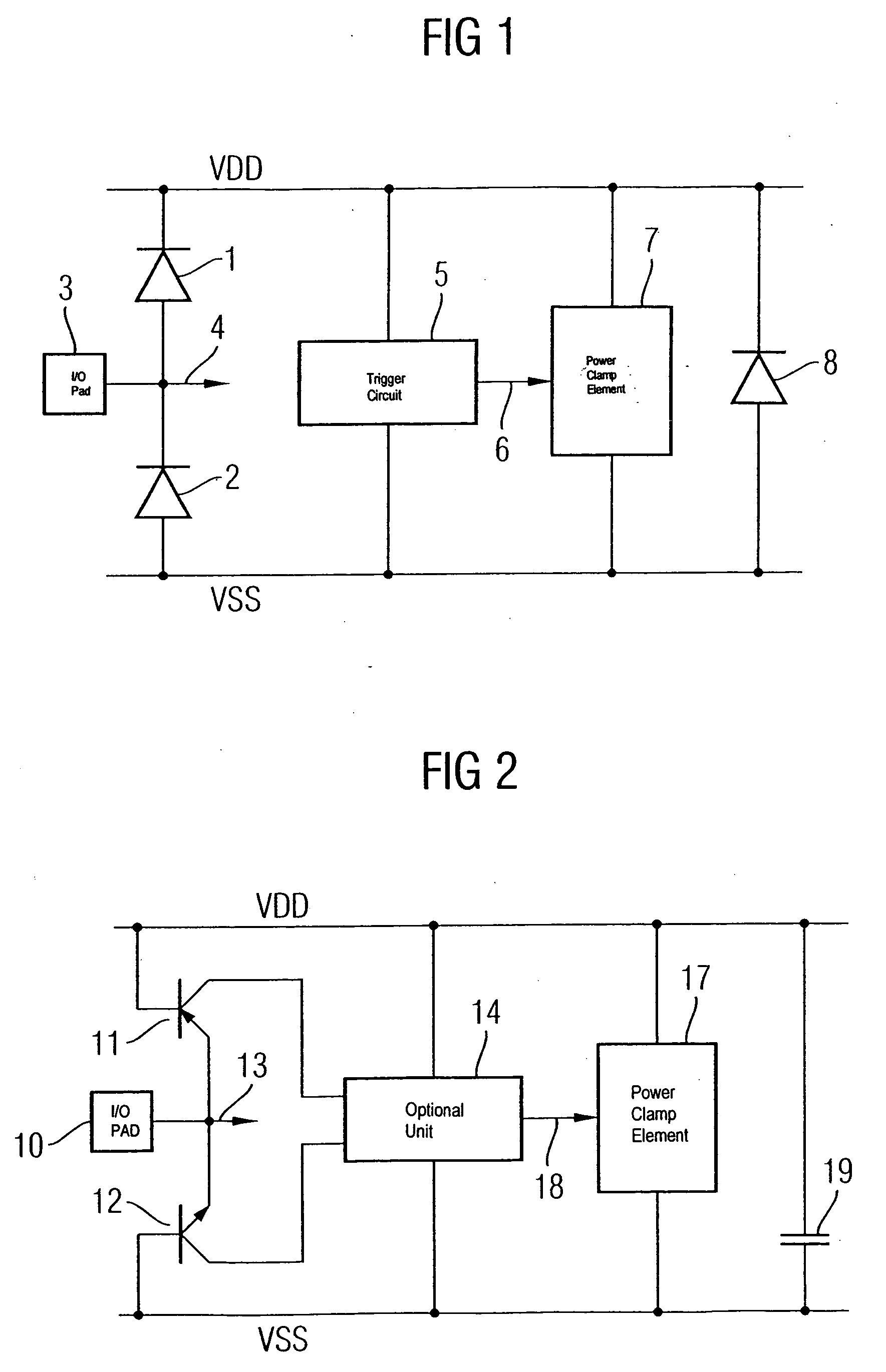
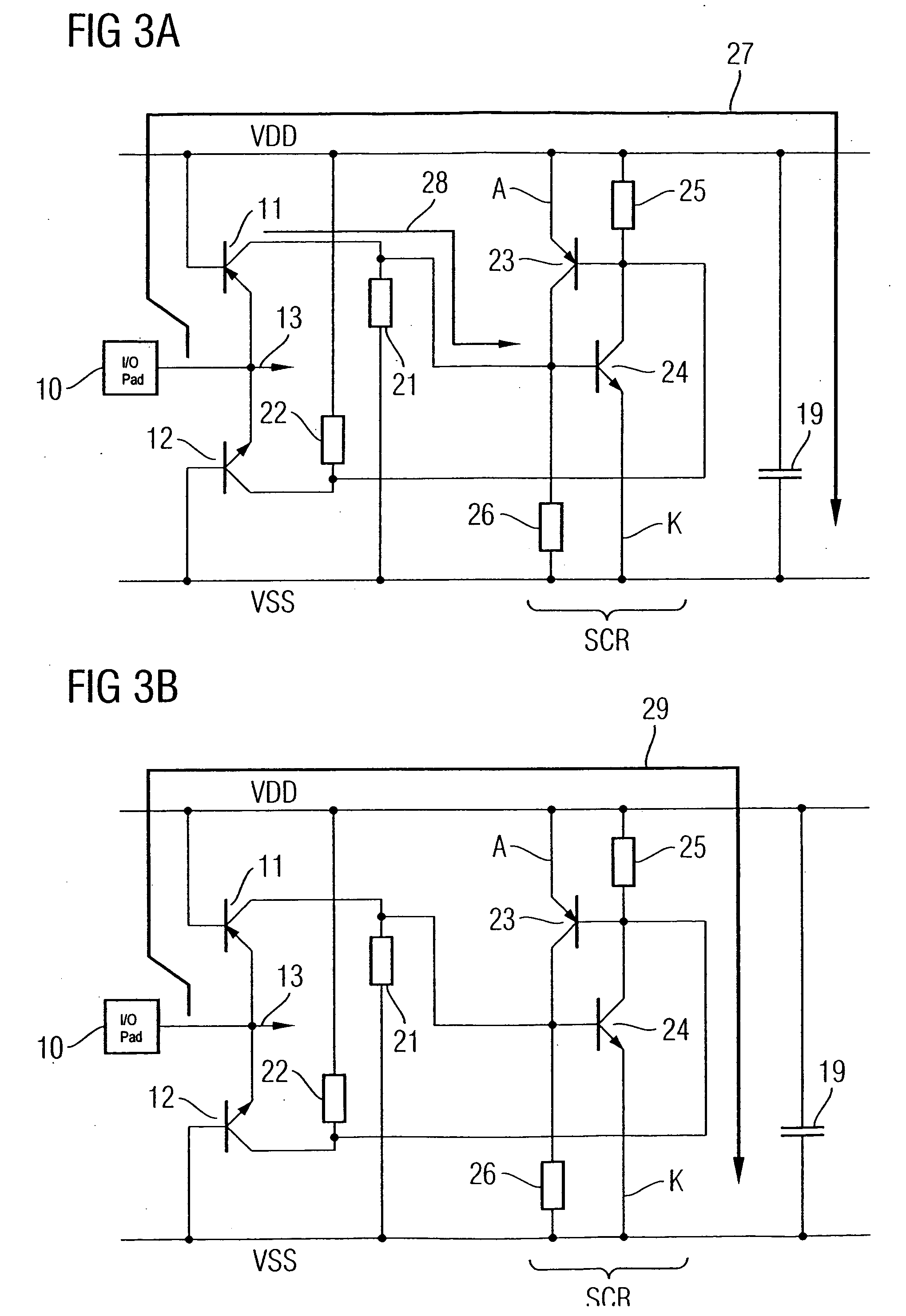
[0048]FIG. 2 illustrates an ESD protective circuit according to one embodiment of the invention. One difference from the ESD protective circuit shown in FIG. 1 is that the diodes 1 and 2 are in the form of base-emitter diodes of two bipolar transistor structures 11 and 12. The pnp transistor structure 11 is in this case electrically connected on the emitter side to the I / O pad 10 to be protected, and on the base side to the VDD network. The npn transistor structure 12 is analogously connected on the emitter side to the pad 10 to be protected, and on the base side to the supply network VSS. The collectors of the pnp transistor structure and of the npn transistor structure are connected to an optional unit 14, which converts the collector current signals to voltage signals, combines them and optionally amplifies them. The unit 14 drives a power clamp element 17 via the signal 18. Furthermore, a coupling capacitance 19 is connected between the supply networks VDD and VSS, which, by way...


PUM


Abstract

An ESD protective circuit protects an input or output of a monolithically integrated circuit. The ESD protective circuit has at least one bipolar transistor structure and one ESD protective element between two supply networks. The emitter of the bipolar transistor structure is electrically connected to the input or output, while the base is electrically connected to one of the two supply networks. The collector produces a current signal, which is used for triggering of the ESD protective element, when an ESD load occurs at the input or output.

Description

PRIORITY [0001] This application claims the benefit of priority to German Patent Application 10 2004 009 981.2, filed on Mar. 1, 2004, herein incorporated by reference in its entirety. TECHNICAL FIELD [0002] This application relates to an ESD protective circuit for protection of at least one input or output of a monolithically integrated circuit having two supply networks. BACKGROUND [0003] It is known that integrated circuits, in particular integrated circuits based on CMOS (Complementary Metal Oxide Semiconductor) circuit technology, must be protected against damaging electrostatic discharges. The aim in this case is to ensure that, in the case of a network of a circuit which can be electrostatically charged from the outside via a pad, electrostatic charging via a further network which is connected to the external environment can be dissipated via a low impedance to the outside again without any damage to the integrated circuit. This is done by means of ESD (Electrostatic Discharg...

Claims


Application Information

Patent Timeline
Patent Type & Authority Applications(United States)
IPC IPC(8): H01L23/60H02H9/00H02H9/02
CPCH01L27/0262H01L27/0259
Inventor STREIBL, MARTINESMARK, KAIRUSS, CHRISTIANWENDEL, MARTINGOSSNER, HARALD
Owner INFINEON TECH AG
Why Eureka
Try Eureka