Nonvolatile semiconductor memory device

a semiconductor memory and non-volatile technology, applied in the direction of instruments, printing, other printing devices, etc., can solve the problems of subject memory cells not being driven, local bit line selection is disabled, and dislocation might occur, so as to reduce the pitch of bit lines and high production yield

Inactive Publication Date: 2005-09-08
RENESAS TECH CORP
View PDF7 Cites 6 Cited by
  • Summary
  • Abstract
  • Description
  • Claims
  • Application Information

AI Technical Summary

Benefits of technology

[0014] (1) In a memory cell forming process, the surface of the isolation trench is oxidized, and the cubic volume of the trench increases during a thermal oxidation treatment performed after the isolation trench is formed. As a result, dislocation might occur due to stress at the boundary between an insulator film and the semiconductor substrate. And, if such dislocation occurs, the select transistor is punched through, with the result that local bit line selection is disabled and the subject memory cells cannot be driven. Both the reliability and the production yield of the flash memory are thus lowered.
[0017] It is another object of the present invention to provide a technique that can improve the reliability of the nonvolatile semiconductor memory device.
[0022] Each select transistor is isolated from the others by a field shielding transistor, thereby the occurrence of dislocation in the select transistor is suppressed. This is why a high production yield is realized for the nonvolatile semiconductor memory device, even when the memory cells are disposed in a highly integrated, manner by reducing the pitch of the bit lines.

Problems solved by technology

If the shallow groove isolation (SGI) method as disclosed in the patent document 3 is used to form the select transistor regions of a flash memory, however, the following problems arise as the isolation width is narrowed more and more.
As a result, dislocation might occur due to stress at the boundary between an insulator film and the semiconductor substrate.
And, if such dislocation occurs, the select transistor is punched through, with the result that local bit line selection is disabled and the subject memory cells cannot be driven.
This makes it difficult to employ the trench isolation method for isolation.

Method used


Image

  • Nonvolatile semiconductor memory device
  • Nonvolatile semiconductor memory device
  • Nonvolatile semiconductor memory device

Examples


first embodiment

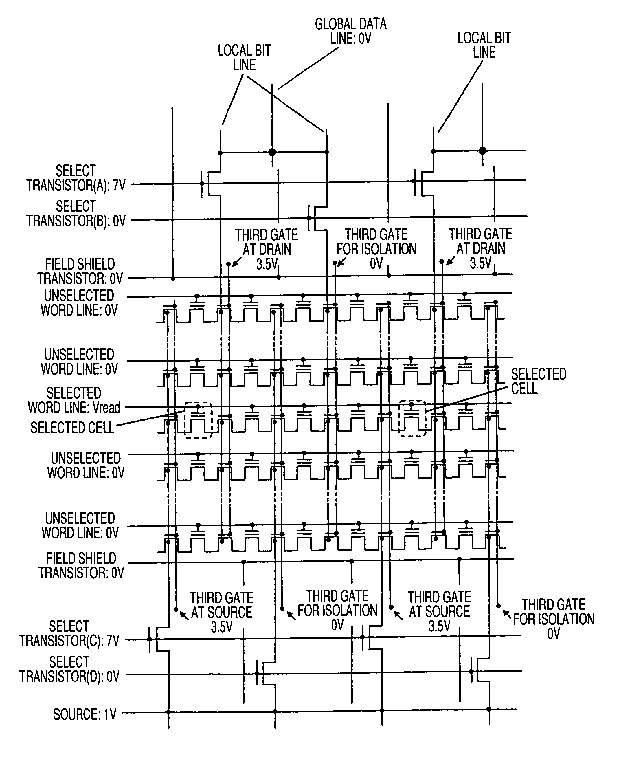
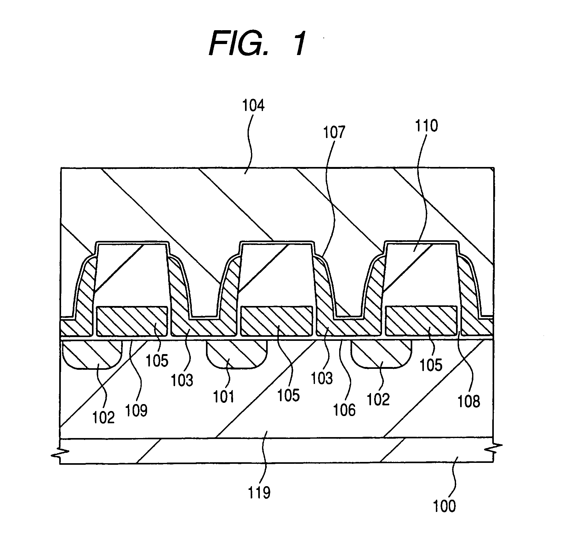
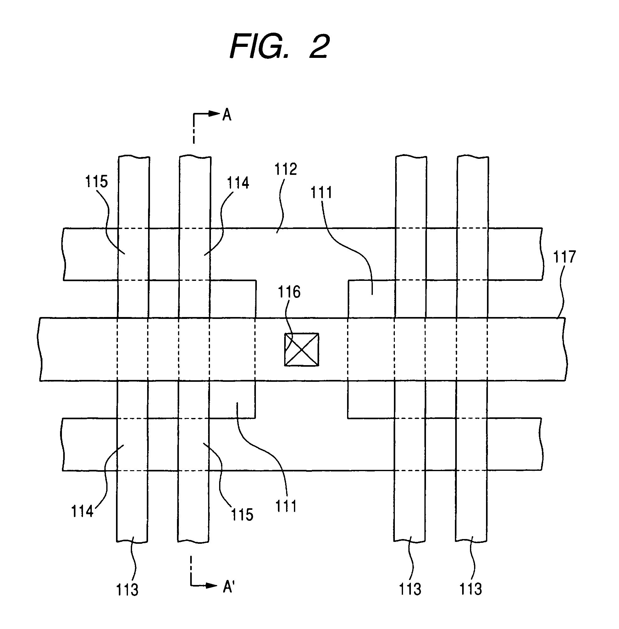
[0057]FIG. 4 shows a partial top view of a semiconductor substrate of a nonvolatile semiconductor memory device in accordance with the first embodiment. FIGS. 5 through 7 show cross sectional views of the semiconductor substrate along the line A-A′, the line B-B′, and the line C-C′in FIG. 4, respectively.

[0058] The nonvolatile semiconductor memory device in this first embodiment has memory cells of a so-called flash memory. In the select transistor region adjacent to each memory cell region, a gate 223 of a field shielding transistor is formed. Between the gates 223 of adjacent field shielding transistors, a gate 224 of a select transistor is disposed in two steps so as to correspond to each transistor. The two steps of the gate 224 are connected to each other by a wiring 226 through a contact hole 225 (FIGS. 4 and 5). The gate 223 of each field shielding transistor is insulated from both of the first conductive type first semiconductor region (well) 201 and the first conductive ty...


PUM


Abstract

A nonvolatile semiconductor memory device to be manufactured at a high production yield has memory cells disposed in a highly integrated manner by suppressing the occurrence of dislocation typically caused by such highly integrated disposition of the memory cells. In order to achieve is result, each field shielding transistor is formed in a select transistor region having a small isolation width, and 0 V is applied to a gate of the field shielding transistor to isolate each local bit line from the others. The gate of each field shielding transistor is connected to another one with a gate member, so that the layout area is reduced more than when a contact hole is provided directly at the gate of each field shielding transistor.

Description

CLAIM OF PRIORITY [0001] The present application claims priority from Japanese application JP 2004-057662, filed on Mar. 2, 2004, the content of which is hereby incorporated by reference into this application. FIELD OF THE INVENTION [0002] The present invention relates in general to a nonvolatile semiconductor memory device; and, more particularly, the invention relates to a technique to be applied effectively to form highly integrated flash memories and to improve the production yield of the same. BACKGROUND OF THE INVENTION [0003] A flash memory is a well-known electrically rewritable nonvolatile semiconductor memory device that enables data to be erased from its memory cells collectively. The flash memory has excellent portability and shock resistance. In recent years, the market for such flash memories has been rapidly expanding, since they are usable as file memory devices in compact portable information devices, such as portable personal computers, digital still cameras, etc. ...

Claims


Application Information

Patent Timeline
Patent Type & Authority Applications(United States)
IPC IPC(8): H01L21/8247B41J29/38G11C7/02H01L27/115H01L29/788H01L29/792
CPCH01L27/11524H10B41/35
Inventor ARIGANE, TSUYOSHIKOBAYASHI, TAKASHISASAGA, YOSHITAKA
Owner RENESAS TECH CORP
Why Eureka
Try Eureka