Semiconductor laser element having tensile-strained quantum-well active layer
- Summary
- Abstract
- Description
- Claims
- Application Information
AI Technical Summary
Benefits of technology
Problems solved by technology
Method used
Image
Examples
Embodiment Construction
[0023] An embodiment of the present invention is explained in detail below with reference to drawings.
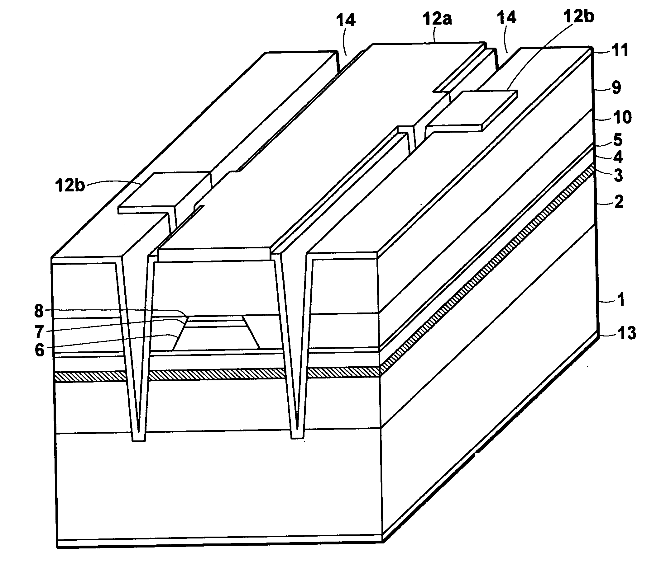
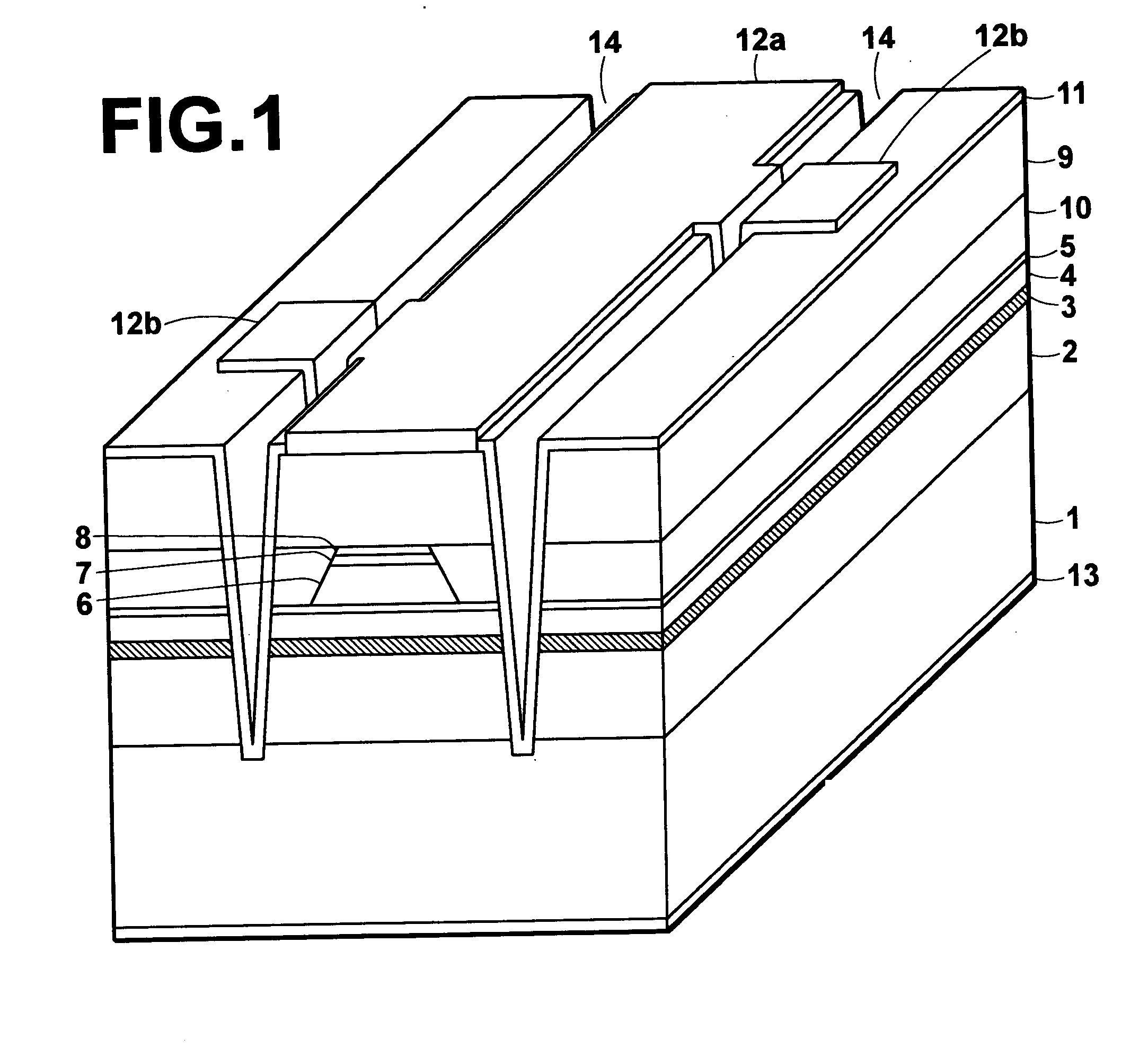
[0024]FIG. 1 is a schematic perspective view of the semiconductor laser element according to the embodiment of the present invention.
[0025] The semiconductor laser element according to the present embodiment is produced by forming a laser structure on an n-type GaAs substrate 1 having a principal plane the crystal orientation of which is tilted 15 degrees from (100) toward (011).
[0026] As illustrated in FIG. 1, the semiconductor laser element according to the present embodiment has a structure in which an n-type (AlxGa1-x)0.5In0.5P lower cladding layer 2 (x=0.7), a light-emission layer 3, a p-type (AlxGa1-x)0.5In0.5P first upper cladding layer 4 (x=0.7), and a p-type InGaP etching-stop layer 5 are formed in this order on the n-type GaAs substrate 1. It is preferable that the p-type InGaP etching-stop layer 5 is a tensile-strain InGaP layer so that the waveguide loss is reduced.
[...
PUM
 Abstract
Description
Claims
Application Information


