
Exposure apparatus and method

a technology of exposure apparatus and mask, which is applied in the direction of photomechanical equipment, instruments, originals for photomechanical treatment, etc., can solve the problems of difficult manufacture of masks provided with phase shifters and difficult arrangement of phase shifters, so as to reduce diffraction components, improve the quantity of light, and minimize the loss of diffracted light

Inactive Publication Date: 2005-09-08
RENESAS ELECTRONICS CORP
View PDF4 Cites 0 Cited by
  • Summary
  • Abstract
  • Description
  • Claims
  • Application Information

AI Technical Summary

Benefits of technology

[0010] It is a further object of the present invention to provide an exposure method and system, and particularly an excimer exposure method and system, in which data of a transferred pattern on a substrate actually transferred by an exposure apparatus can be confirmed through simulation by arithmetic processing.
[0011] It is another object of the present invention to provide a mask circuit pattern inspection system in which even in the case where an extremely fine circuit pattern formed on a mask is different from a pattern transferred onto a substrate, the extremely fine circuit pattern formed on the mask can be inspected with high accuracy.
[0025] In order to minimize the loss of the diffracted light, it is contemplated that the wavelength is shortened to reduce diffraction components as in an excimer laser stepper or the NA of the imager (projection lens) is increased so as to receive diffraction light as much as possible.
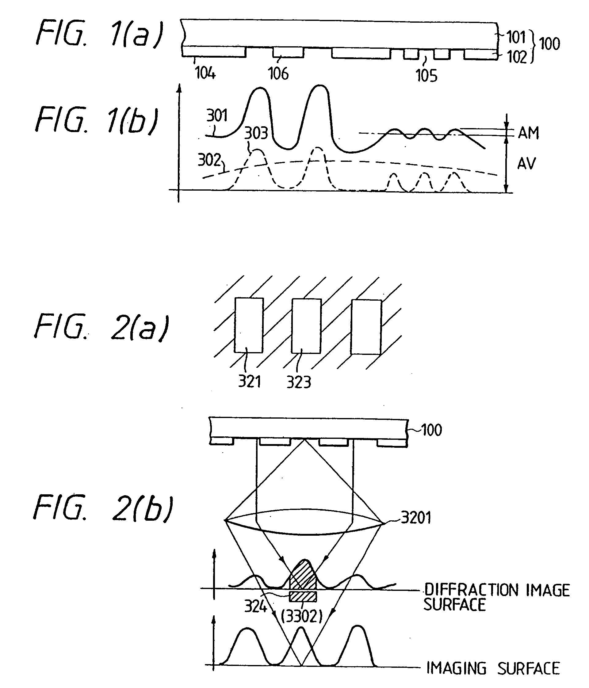
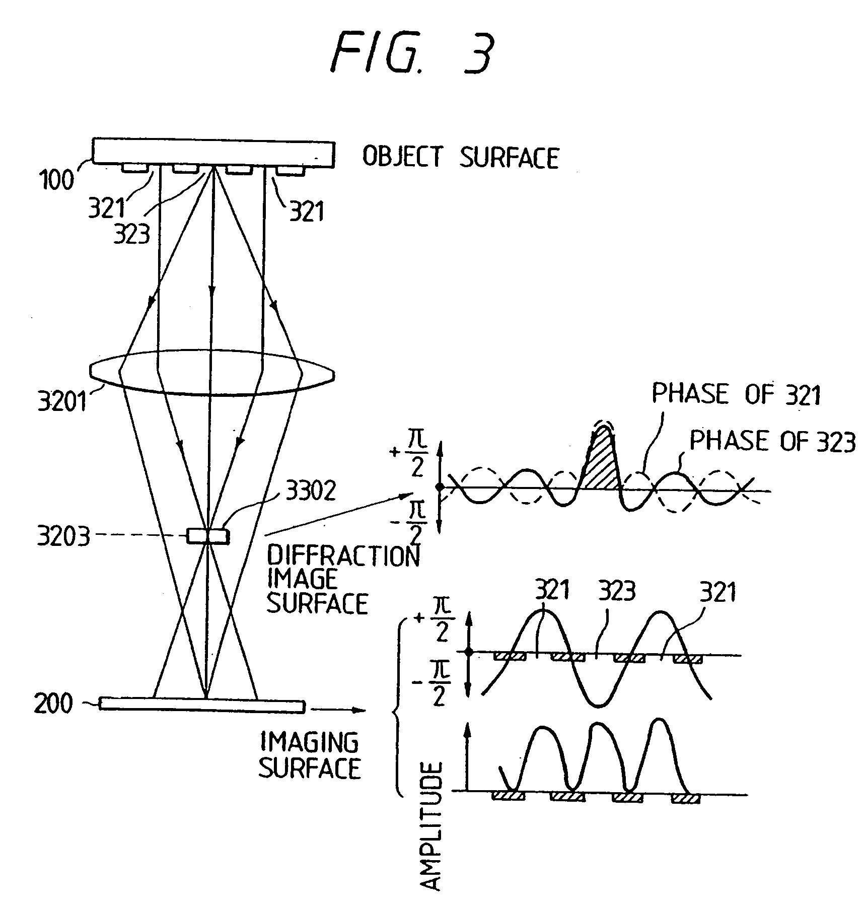
[0026] On the other hand, according to the present invention, with a view to a phenomenon in which less components of diffraction light from a circuit pattern on a mask is received into imager (projection lens) whereas all components (O-order diffraction light) not diffracted from the circuit pattern on the mask are received therein, the O-order diffraction light alone in a large amount of light necessary for imaging is received into the imager (projection lens), and less diffraction light components is relatively received into the imager (projection lens). From a viewpoint of this, at least a part of the O-order diffraction light is shielded thereby to relatively improve a balance in quantity of light between the diffraction light emitted out of the imager (projection lens) and the O-order diffraction light and to improve the contrast of an extremely fine circuit pattern formed on the mask to be imaged and transferred onto the substrate through the imager (projection lens), thus realizing the exposure with high resolving power.
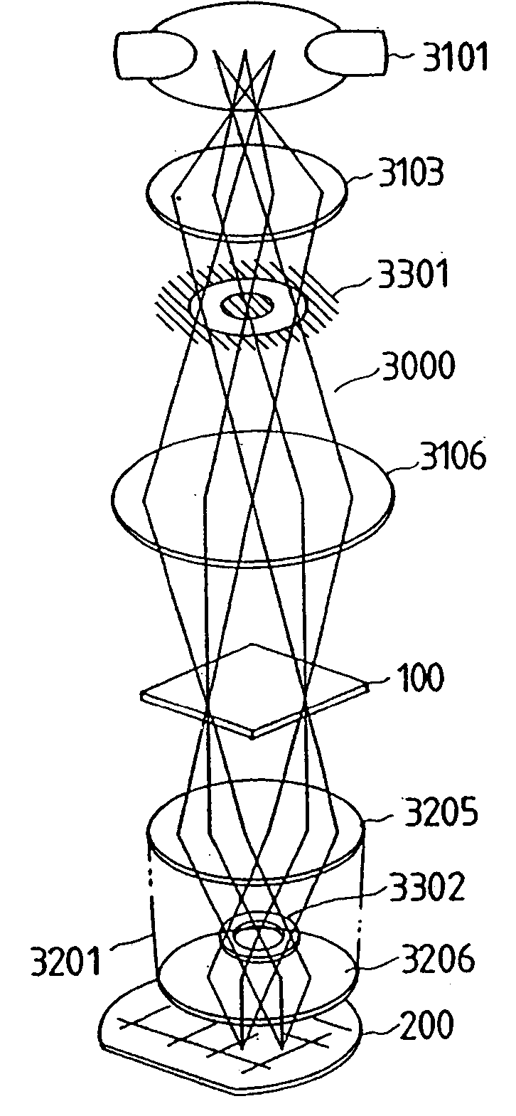
[0027] Particularly, in the present invention, there are provided an illuminating arrangement for substantially uniformly applying a ring-like diffused illumination formed from a number of imaginary point sources to a mask in an exposure area, and a reduction projection lens having an optical aye which shields at least a part of the O-order diffraction light or low-order diffraction light out of light which transmits through the mask substantially uniformly diffused and illuminated by the illuminating arrangement and imaging a circuit pattern formed on said mask on a substrate in the exposure area. With this structure, an extremely fine circuit pattern formed on the mask is imaged and transferred onto the substrate through the reduced projection lens to improve the contrast, thus realizing an exposure of high resolving power.

Problems solved by technology

However, to cope with the need of high integration of LSI, the circuit pattern transferred onto the wafer tends to be an extremely fine pattern, which constitutes a resolution limit of an imaging optical system.
However, the prior art known from the aforementioned Patent Publication No. 62(1987)-50811 has a problem in that an arrangement of the phase shifter is difficult, and the manufacture of a mask provided with the phase shifter is difficult.

Method used


Image

  • Exposure apparatus and method
  • Exposure apparatus and method
  • Exposure apparatus and method

Examples


Embodiment Construction

[0080] First, the principle of the present invention will be described with reference to FIGS. 1 to 7. In the present invention, a circuit pattern on a mask is transferred with an improved contrast rather than the art in which the circuit pattern is faithfully transferred onto a substrate by the imager (projection lens). Namely, in projection exposure, the requirement that “a circuit pattern is transferred accurately” is not always necessary the present invention is based on a new technical feature that “a circuit pattern desirably formed on a substrate (wafer) is better transferred with high contrast”.

[0081]FIG. 1(a) is a sectional view of a mask 100 in which a mask circuit pattern 104 is formed on a glass substrate 101 by chrome 102. In FIG. 1(b), a waveform 301 shows, with respect to the mask circuit pattern 104, a signal distribution of an imaging pattern imaged onto a substrate (wafer) 200 by a projection and exposure device 3000 as shown in FIGS. 4 to 6. The waveform 301 is d...


PUM

PropertyMeasurementUnit
widthaaaaaaaaaa
wavelengthaaaaaaaaaa
transmittanceaaaaaaaaaa

Abstract

A production method of a semiconductor device which includes the steps of exposing a resist coated on a substrate of a semiconductor device by projecting a light pattern on the substrate of the semiconductor device, developing the resist exposed by the light pattern to form a wafer pattern with the resist, and etching the substrate on which the wafer pattern with the resist is formed. In the step of exposing the light pattern is formed by illuminating a mask with excimer laser light having an annular shape.

Description

CROSS REFERENCE TO RELATED APPLICATIONS [0001] This is a continuation of U.S. application Ser. No. 10 / 282,081, filed Oct. 29, 2002, which is a continuation of U.S. application Ser. No. 09 / 542,072, filed Apr. 3, 2000, now U.S. Pat. No. 6,485,891, which is copending with U.S. application Ser. No. 09 / 542,071, filed Apr. 13, 2000, now U.S. Pat. No. 6,335,146, which are continuations of U.S. application Ser. No. 09 / 447,243, filed Nov. 23, 1999, which is a continuation of U.S. application Ser. No. 09 / 003,141, filed Jan. 6, 1998, now U.S. Pat. No. 6,016,187, issued Jan. 18, 2000, which is a continuation of U.S. application Ser. No. 08 / 727,762, filed Oct. 8, 1996, now U.S. Pat. No. 5,767,949, issued Jun. 16, 1998, which is a continuation of U.S. application Ser. No. 08 / 501,178, filed Jul. 11, 1995, now abandoned, which is a continuation of U.S. application Ser. No. 08 / 235,654, filed Apr. 29, 1994, now U.S. Pat. No. 5,526,094, issued Jun. 11, 1996, which is a continuation of U.S. application...

Claims


Application Information

Patent Timeline
Patent Type & Authority Applications(United States)
IPC IPC(8): G03F1/84G03F7/20H01L21/027H01L21/30
CPCG03F7/2002G03F7/701G03F7/70125Y10S430/146G03F7/705G03F7/70591G03F7/70308
Inventor NOGUCHI, MINORIKENBO, YUKIOOSHIDA, YOSHITADASHIBA, MASATAKAYOSHITAKA, YASUHIROMURAYAMA, MAKOTO
Owner RENESAS ELECTRONICS CORP
Learn More