Method of forming stress-relaxed SiGe buffer layer

a buffer layer and stress-relaxed technology, applied in the direction of basic electric elements, electrical equipment, semiconductor devices, etc., can solve the problems of shortening the process time, degrading device characteristics or generating leakage current, and affecting the quality of the product, so as to reduce the density of surface dislocation and small thickness

Inactive Publication Date: 2005-09-08
ELECTRONICS & TELECOMM RES INST
View PDF7 Cites 34 Cited by
  • Summary
  • Abstract
  • Description
  • Claims
  • Application Information

AI Technical Summary

Benefits of technology

[0021] The present invention is also directed to a method of forming a stress-relaxed SiGe buffer layer which has a relatively small thickness, a reduced surface dislocation density, and a surface roughness similar to bulk silicon.

Problems solved by technology

Third, the misfit dislocation which may occur while the stress is relaxed should not be propagated to a surface of the buffer layer.
Dislocation which is propagated to the surface of the buffer layer may serve as a defect in an active device formed thereon to thereby degrade device characteristics or generate a leakage current.
However, the composition variation growth method has disadvantages in that a deposition process time is lengthened, which leads to the low manufacturing yield and surface roughness is tens of nano meters which is too rough to be practically applied to a device since a thickness more than several micrometers is required.
Most of cases form defects at an interface and use the defects as a source of forming the misfit dislocation.
However, this method is also difficult to be practically applied to a device because a low temperature silicon layer should be grown by the MBE method.
However, this method cannot also obtain a satisfactory result.

Method used


Image

  • Method of forming stress-relaxed SiGe buffer layer
  • Method of forming stress-relaxed SiGe buffer layer
  • Method of forming stress-relaxed SiGe buffer layer

Examples


Embodiment Construction

[0037] Exemplary embodiments of the present invention will now be described more fully with reference to the accompanying drawings. This invention may, however, be embodied in different forms and should not be construed as limited to the embodiments set forth herein. Rather, these embodiments are provided so that this disclosure will be thorough and complete, and will fully convey the scope of the invention to those skilled in the art.

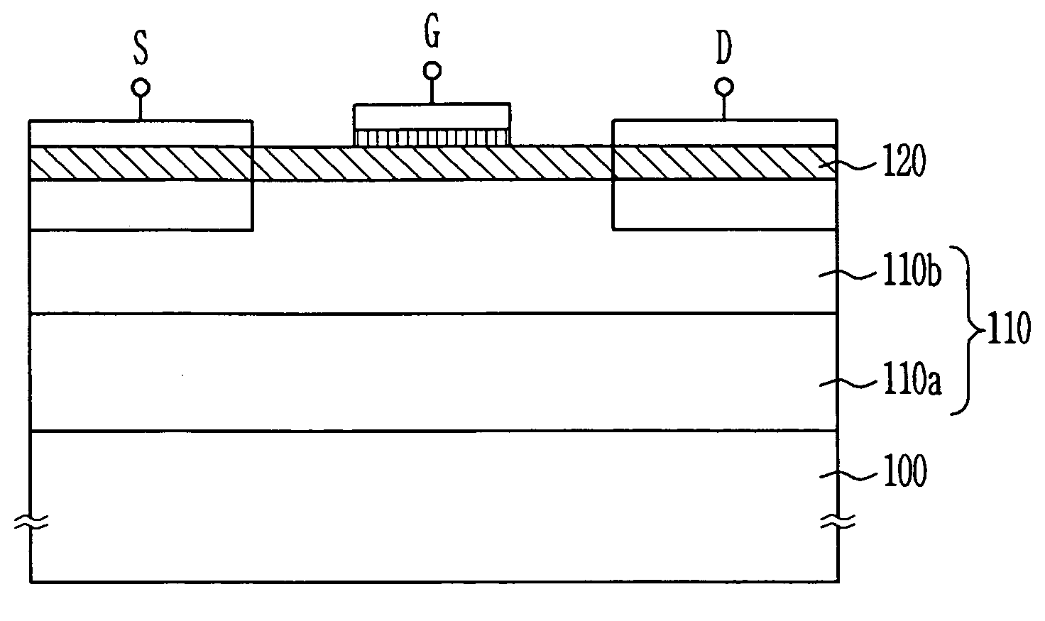
[0038]FIG. 1 is a cross-sectional view illustrating a silicon-based MOS transistor which employs a SiGe buffer layer in accordance with the present invention.

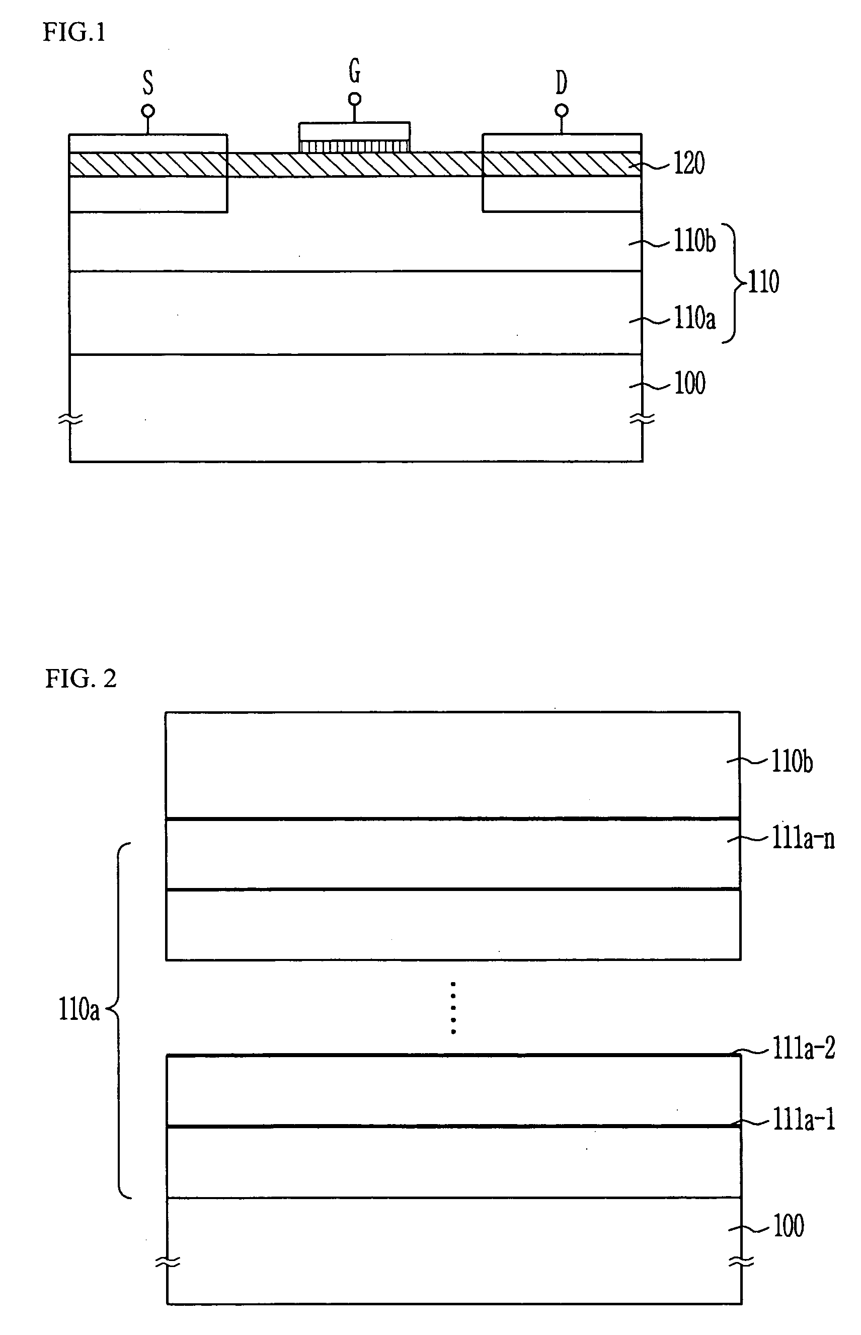
[0039] A SiGe buffer layer 110 including a graded composition layer, i.e., a graded Si1-xGex layer 110a and a constant composition layer, i.e., constant Si1-yGey layer 110b which are formed on a silicon substrate 100. A gate of a MOS transistor is formed above the SiGe buffer layer 110, and a source S and a drain D are formed in both sides of the SiGe buffer layer 110, and a tensily strained sil...


PUM

PropertyMeasurementUnit
temperatureaaaaaaaaaa

Abstract

Provided is a method of forming a stress-relaxed SiGe buffer layer on a silicon substrate using a reduced pressure chemical vapor deposition (RPCVD) technique. The method includes: forming a graded composition layer having a predetermined germanium composition gradient on a silicon substrate; forming and thermally annealing a first constant composition layer having a predetermined germanium composition on the graded composition layer; removing the first constant composition layer by a predetermined thickness to planarize a surface; and forming a second constant composition layer on the first constant composition layer to form a SiGe buffer layer having the graded composition layer and the constant composition layer. A strained silicon or SiGe channel can be formed in a silicon-based MOSFET device or a MODFET device by forming the stress-relaxed SiGe buffer layer that has a relatively thin thickness, a low surface dislocation density, and a surface roughness similar to bulk silicon, and thus a device having excellent channel conductivity and high frequency characteristics can be manufactured.

Description

CROSS-REFERENCE TO RELATED APPLICATION [0001] This application claims priorities to and the benefit of Korean Patent Application Nos. 2003-98046 and 2004-16498, filed Dec. 22, 2003 and Mar. 11, 2004, the disclosure of which are incorporated herein by reference in its entirety. BACKGROUND [0002] 1. Field of the Invention [0003] The present invention relates to a method of forming a silicon-germanium (SiGe) buffer layer and, more particularly, to a method of forming a stress-relaxed SiGe buffer layer which can be applied to the manufacture of a modulation doped field effect transistor (MODFET) or a metal oxide semiconductor field effect transistor (MOSFET) which uses a Si / SiGe heterojunction. [0004] 2. Discussion of Related Art [0005] Researches on a device having a Si / SiGe heterojunction structure have been performed for the past several decades. According to research results, it is known that electron mobility in a tensily strained Si channel formed on a SiGe single crystal is highe...

Claims


Application Information

Patent Timeline
Patent Type & Authority Applications(United States)
IPC IPC(8): H01L29/739
CPCH01L21/02381H01L21/0245H01L21/0251H01L21/02532H01L29/165H01L29/7782H01L29/78H01L29/1054H01L21/0262
Inventor KIM, SANG HOONSHIM, KYU HWANKANG, JIN YEONG
Owner ELECTRONICS & TELECOMM RES INST
Why Eureka
Try Eureka