Heterojunction bipolar transistor and manufacturing method thereof

Inactive Publication Date: 2005-09-15
COLLABO INNOVATIONS INC
View PDF3 Cites 13 Cited by
  • Summary
  • Abstract
  • Description
  • Claims
  • Application Information

AI Technical Summary

Benefits of technology

[0032] According to this method, the base electrode is formed on the second emitter layer which is made of InGaP so as to come in ohmic contact with the base layer, which allows reduction of the recombination current in the base. Therefore, it is possible to realize a manufacturing method of a heterojunction bipolar transistor with high performance and high reliability.
[0033] As is clear from the above description, according to the present invention, it is possible to realize a heterojunction bipolar transisto

Problems solved by technology

However, there is a problem that a conventional InGaP/G

Method used


Image

  • Heterojunction bipolar transistor and manufacturing method thereof
  • Heterojunction bipolar transistor and manufacturing method thereof
  • Heterojunction bipolar transistor and manufacturing method thereof

Examples


first embodiment

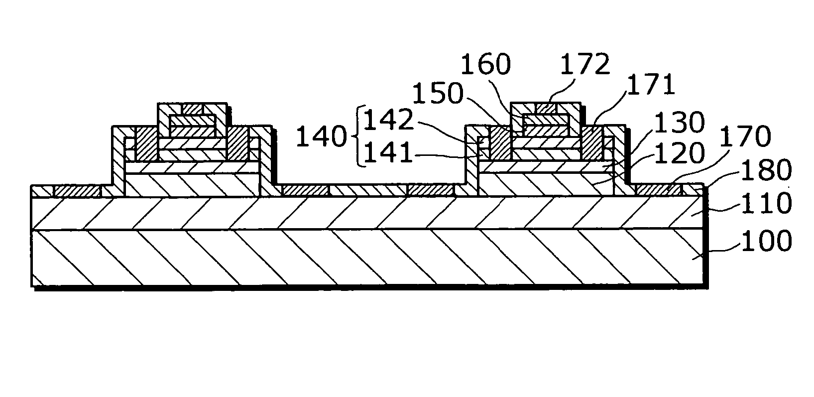
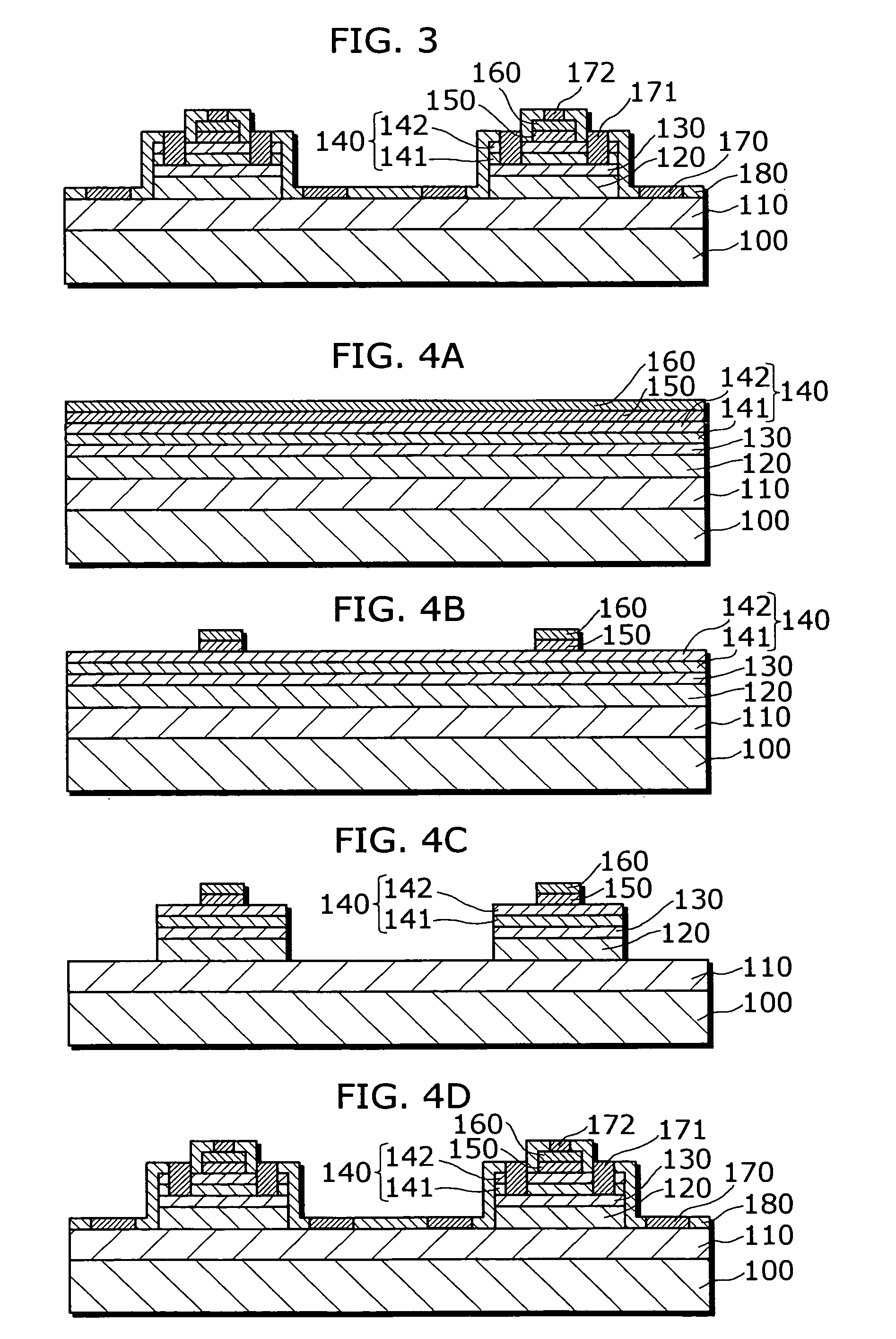
[0047]FIG. 3 is a cross-sectional view showing a structure of the HBT in the first embodiment.

[0048] The HBT of the present embodiment aims at realizing an HBT having improved breakdown voltage on operation for high power output. This HBT has a multilayer structure including the following layers formed on a semi-insulating GaAs semiconductor substrate 100 in the following order: an n+-type GaAs sub-collector layer 110 formed by doping an n-type dopant with high concentration; an n-type GaAs collector layer 120 with low dopant concentration; a p-type GaAs base layer 130 formed by doping a p-type dopant such as C with high concentration; an emitter layer 140; an n-type GaAs emitter cap layer 150; and an n-type InGaAs emitter contact layer 160 for forming an emitter electrode with low contact resistance.

[0049] The emitter layer 140 includes a first emitter layer 141 and a second emitter layer 142 which are laminated on the base layer 130 in this order. Here, the first emitter layer 1...

second embodiment

[0065]FIG. 6 is a cross-sectional view showing a structure of the HBT in the second embodiment. The same reference numbers are assigned to the same components as those in FIG. 3, and the detailed explanation thereof is not repeated here.

[0066] The HBT in the present embodiment has a multilayer structure including the following layers formed on the semiconductor substrate 100 in the following order: the sub-collector layer 110; the collector layer 120; the base layer 130; and an emitter layer 400; the emitter cap layer 150; and the emitter contact layer 160.

[0067] The emitter layer 400 includes a second emitter layer 401 and a first emitter layer 402 which are laminated on the base layer 130 in this order. Here, the second emitter layer 401 is an n-type layer which is made of InxGa1-xP with In composition of about 50%, while the first emitter layer 402 is a non-doped or n-type layer which is made of a semiconductor material including Al. Here, the semiconductor material including A...

third embodiment

[0079]FIG. 8 is a cross-sectional view showing a structure of the HBT in the third embodiment. The same reference numbers are assigned to the same components as those in FIG. 3, and the detailed explanation thereof is not repeated here.

[0080] The HBT of the present embodiment has a multilayer structure including the following layers formed on the semiconductor substrate 100 in the following order: the sub-collector layer 110; the collector layer 120; the base layer 130; and an emitter layer 600; the emitter cap layer 150; and the emitter contact layer 160.

[0081] The emitter layer 600 includes a first emitter layer 601 and a second emitter layer 602, which is formed on the first emitter layer 601 and the base layer 130, covering the first emitter layer 601. Here, the first emitter layer 601 is a non-doped or n-type layer which is made of a semiconductor material including Al, while the second emitter layer 602 is an n-type layer, with the thickness of 20 to 50 nm, which is made of ...


PUM


Abstract

The present invention aims at providing a heterojunction bipolar transistor having improved breakdown voltage on operation for high power output, and includes: a GaAs semiconductor substrate 100; an n+-type GaAs sub-collector layer 110; an n-type GaAs collector layer 120; a p-type GaAs base layer 130; an emitter layer 140; an n-type GaAs emitter cap layer 150; and an n-type InGaAs emitter contact layer 160. The emitter layer 140 has a multilayer structure including an n-type or non-doped first emitter layer 141 and an n-type second emitter layer 142 which are laminated in sequence. The first emitter layer 141 is made of a semiconductor material including Al, while the second emitter layer 142 is made of InxGa1-xP (0<x<1).

Description

BACKGROUND OF THE INVENTION [0001] (1) Field of the Invention [0002] The present invention relates to a heterojunction bipolar transistor and its manufacturing method. [0003] (2) Description of the Related Art [0004] A heterojunction bipolar transistor (hereinafter referred to as HBT) using a semiconductor of a large bandgap as an emitter has gained attention as a high-frequency analogue device used for a cell phone and the like. Particularly, an InGaP / GaAs HBT using InGaP as an emitter has been commercially utilized as a device with high performance and high reliability because it has the following advantages: lower dependency on temperature of a current amplification factor (HFE) because of large valence band discontinuity (ΔEv); and less recombination current in the base because of no existence of the interface trapped density nor the DX center (See, for example, Japanese Laid-Open Patent Application Publication H5-36713 and Japanese Laid-Open Patent Application Publication H8-24...

Claims


Application Information

Patent Timeline
IPC IPC(8): H01L21/331H01L29/205H01L29/737H01L29/739
CPCH01L29/0817H01L29/7371H01L29/66318
Inventor MURAYAMA, KEIICHIOTA, YORITOTAMURA, AKIYOSHI
Owner COLLABO INNOVATIONS INC
Why Eureka
Try Eureka