
Method for implementing base region window of silicon germanium heterojunction transistor

A technology of heterojunction transistors and base regions, which is applied in the direction of semiconductor devices, semiconductor/solid-state device manufacturing, electrical components, etc., can solve the problems of discontinuous metal silicide, increased resistance of the outer base region, and insufficient insulation. Achieve the effect of eliminating sidewall residue, reducing base resistance, and reducing defects

Active Publication Date: 2013-03-13
SHANGHAI HUAHONG GRACE SEMICON MFG CORP
View PDF0 Cites 0 Cited by
  • Summary
  • Abstract
  • Description
  • Claims
  • Application Information

AI Technical Summary

Problems solved by technology

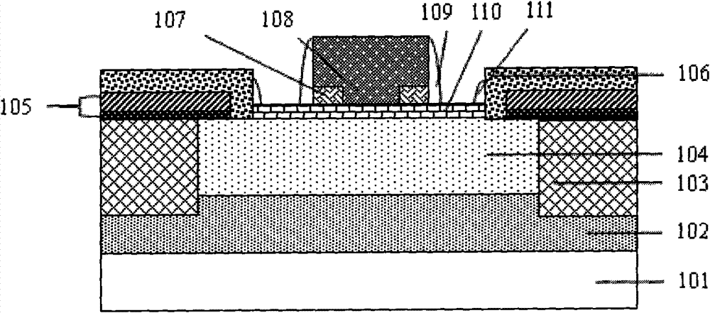
When the process steps of the sidewall 109 are implemented, the insulating sidewall 111 will also be formed on the step at the window interface of the base region, so that the formation of the metal silicide is discontinuous here, resulting in an increase in the resistance of the outer base region and affecting device performance.
Removing the insulating spacer 111 at the step by over-etching is a potential risk. To avoid the influence of the thermal budget on device performance after SiGe is formed, the film used for the insulating spacer 111 is usually an oxide film formed by plasma. , excessive etching will lead to insufficient thickness of the sidewall between the emitter and the base, which is not enough to achieve insulation

Method used


Image

  • Method for implementing base region window of silicon germanium heterojunction transistor
  • Method for implementing base region window of silicon germanium heterojunction transistor
  • Method for implementing base region window of silicon germanium heterojunction transistor

Examples


Embodiment Construction

[0020] The method for realizing the base region window of the silicon-germanium heterojunction transistor described in the present invention is to deposit a layer of dielectric film layer after the dielectric film is partially opened and before the oxide film is removed, and use the dielectric film layer to form a step in the base region window interface. A D-shaped side wall is formed; at the same time, using the protection of the D-shaped side wall, the remaining oxide film in the window of the base region is removed by wet method, and the SiGe base region is epitaxially grown in a short time. The formation of the D-shaped sidewall makes the step of the window interface of the base area gradually changed. After SiGe epitaxy, the gradually changed step formed by the D-shaped sidewall remains, so that there is no insulator residue in the subsequent emitter polysilicon sidewall process. In this way, a continuous metal silicide is formed to reduce the resistance of the outer base...


PUM


Abstract

The invention discloses a method for implementing a base region window of a silicon germanium heterojunction transistor, which comprises the following steps of: depositing a composite dielectric film on a silicon chip with an embedded layer, a collector region and a substrate isolation region on a silicon substrate; performing dry etching on the composite dielectric film, defining the base region window, and etching an oxide film stopped on the composite dielectric film; after the base region window is opened and before the oxide film of the composite dielectric film is removed, depositing a dielectric film layer, and forming a D-shaped side wall at the interface step of the base region window by using the dielectric film layer; and meanwhile, performing wet removal on the residual oxide film in the base region window by using the protection of the D-shaped side wall, and epitaxially growing an SiGe base region. The interface step of the base region window is changed slowly because of the formation of the D-shaped side wall, and the slowly changed step formed by the D-shaped side wall is continuously reserved after SiGe extension and has no insulator residue in the subsequent emitter polycrystalline silicon side wall process, so that continuous metal silicide is formed, the resistance of an outer base region is reduced, and the performance of the device is improved.

Description

technical field [0001] The invention relates to the field of semiconductor integrated circuits, in particular to a method for realizing a base region window of a silicon-germanium heterojunction transistor. Background technique [0002] In the manufacturing process of SiGe (silicon germanium) heterojunction transistor (SiGe HBT), the formation of SiGe base region is realized by means of epitaxy, including selective epitaxy, non-selective epitaxy and composite epitaxy. [0003] The current conventional non-selective epitaxial base formation method is (combined with figure 1 shown): 1. Dielectric film 105 deposition. The dielectric film 105 is an oxide film, or a combination of an oxide film and other film qualities. 2. The SiGe base window opens. 3. SiGe epitaxial growth, forming the SiGe base monocrystalline silicon layer 110 and the SiGe outer base region 106, growing monocrystalline silicon in the monocrystalline silicon region, and growing polycrystalline silicon in ot...

Claims


Application Information

Patent Timeline
Patent Type & Authority Patents(China)
IPC IPC(8): H01L21/331H01L21/28
Inventor 陈帆张海芳徐炯
Owner SHANGHAI HUAHONG GRACE SEMICON MFG CORP
Learn More