Device and method for wavefront measurement of an optical imaging system, and a microlithography projection exposure machine

a technology of optical imaging system and exposure machine, which is applied in the field of optical imaging system wavefront measurement device and exposure machine, and the application of microlithography projection exposure machine to achieve the effect of reducing the influence of nonideal periodic structure on measurement and increasing the measuring accuracy

Active Publication Date: 2005-09-15
CARL ZEISS SMT GMBH
View PDF5 Cites 38 Cited by
  • Summary
  • Abstract
  • Description
  • Claims
  • Application Information

AI Technical Summary

Benefits of technology

[0019] In a development of the method according to the invention, the optical element with the object-side structure and/or the optical element with the image-side structure are/is displaced laterally along a periodicity direction in order to produce overlay patterns with a different phase offset, it being possible to increase the measuring accuracy thereby.
[0020] In a development of the method according to the invention, the

Problems solved by technology

However, such a case is not mandatory for the wavefront measurement, that is to say the pupil regions

Method used


Image

  • Device and method for wavefront measurement of an optical imaging system, and a microlithography projection exposure machine
  • Device and method for wavefront measurement of an optical imaging system, and a microlithography projection exposure machine
  • Device and method for wavefront measurement of an optical imaging system, and a microlithography projection exposure machine

Examples


Embodiment Construction

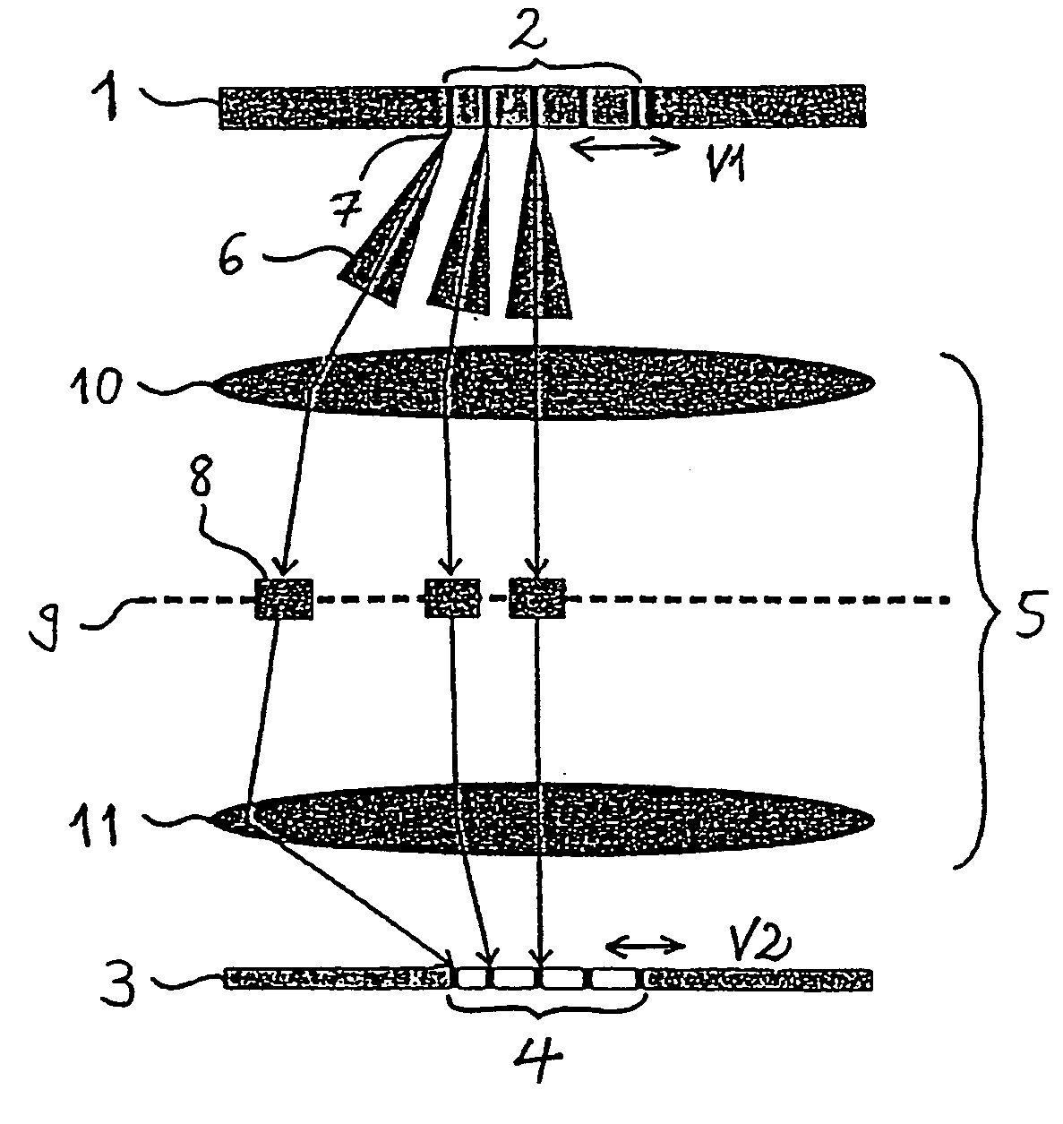
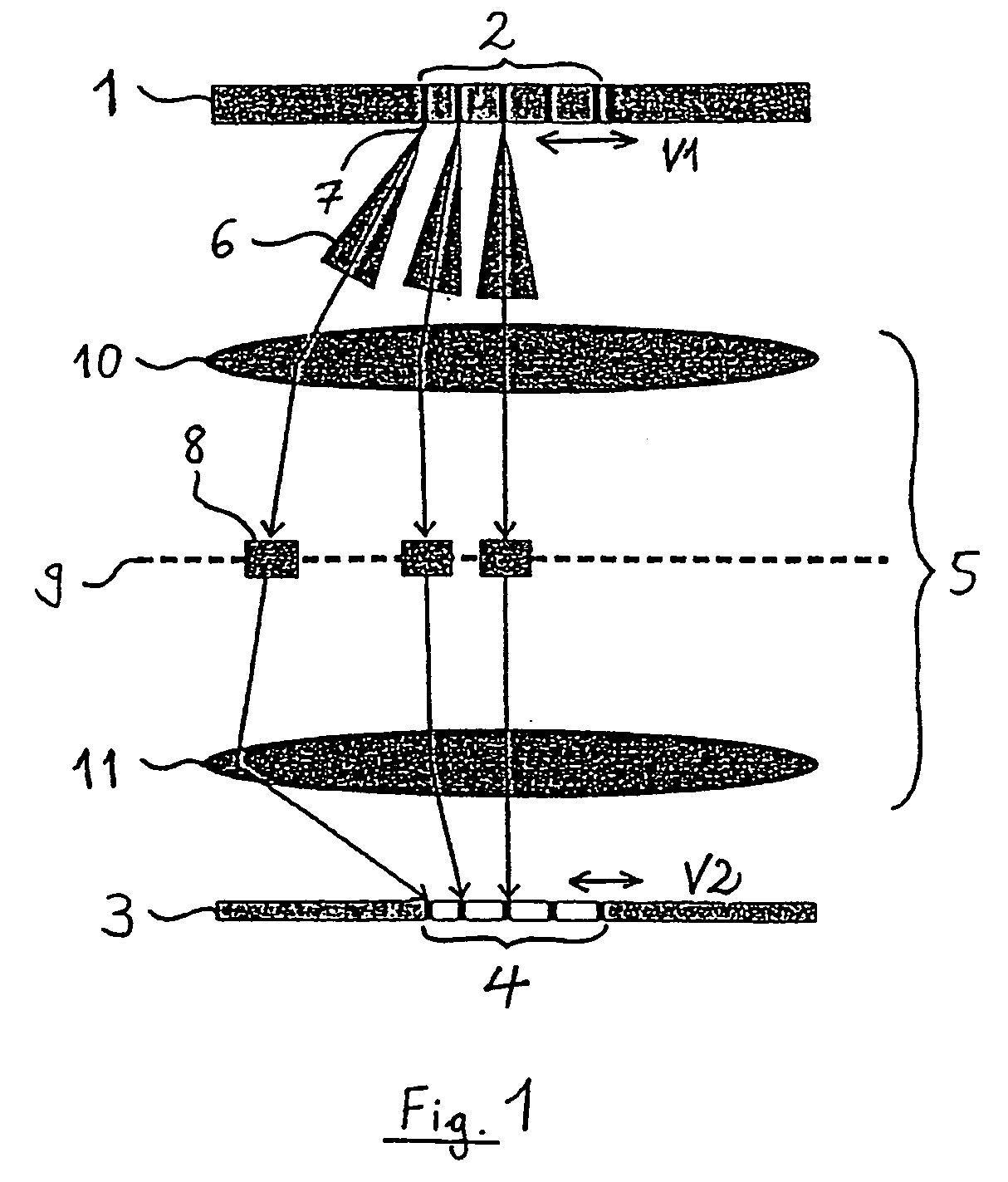
[0034]FIG. 1 shows a schematic of a device according to the invention for wavefront measurement on a projection lens 5 for microlithography, having a measuring reticle 1 that is located in the object plane of the lens 5 and has a first periodic moiré structure 2, and is part of a wavefront generating unit not represented further pictorially. For the sake of simplicity, only a first, entrance-side lens 10 and a second, exit-side lens 11 of the projection lens 5 are shown. The lens 5 projects structures applied to the reticle 1 onto a structure carrier 3 that is placed in the image plane of the lens 5 and has a second periodic moiré structure 4 as part of a detector unit not further represented pictorially.

[0035] The device shown in FIG. 1 for wavefront measurement is integrated in a microlithography projection exposure machine, for example a wafer scanner, in such a way that it is possible to switch over rapidly between the measurement operation and the lithographic exposure operati...


PUM


Abstract

A device and a method for wavefront measurement of an optical imaging system, and a microlithography projection exposure machine that is equipped with such a device. The device has a wavefront generating unit that includes an optical element (1) with an object-side periodic structure (2), and a light source unit (20,21) for illuminating the object-side periodic structure with the aid of a measuring radiation. The device also has a detector unit that is arranged on the image side of the imaging system to be measured and that includes an optical element (3) with an image-side periodic structure, and a detector element (52, 52a, 52b) for detecting an overlay pattern of the imaged object-side periodic structure and image-side periodic structure. The wavefront generating unit is designed to restrict the angular spectrum (6) of the measuring radiation emanating from a respective field point (7), the design being such that the measuring radiation emanating from the respective field point illuminates only in each case a specific subregion of a pupil plane of the optical imaging system.

Description

[0001] This is a Continuation of International Application PCT / EP2004 / 000291, with an international filing date of Jan. 16, 2004, which was published under PCT Article 21(2) in German, and the disclosure of which is incorporated into this application by reference.BACKGROUND OF THE INVENTION [0002] 1. Field of the Invention [0003] The invention relates to a device and a method for wavefront measurement of an optical imaging system, and to a microlithography projection exposure machine having a projection lens and comprising such a device. [0004] 2. Description of the Related Art [0005] Methods and devices for wavefront measurement are used variously for determining aberrations of optical imaging systems, in particular ultra-precision projection lenses in microlithography projection exposure machines. During wavefront measurement, deviation of the surface shape is determined with reference to an ideal surface shape. Such a deviation is denoted as a wavefront abberation. The imaging qu...

Claims


Application Information

Patent Timeline
IPC IPC(8): G02F1/29G03F7/20
CPCG03F7/706G01B9/02
Inventor EMER, WOLFGANG
Owner CARL ZEISS SMT GMBH
Why Eureka
Try Eureka