Magnetoresistive element, magnetic head, and magnetic recording and reproducing apparatus

a technology of magnetic head and element, applied in the field of magnetic head, magnetic recording and reproducing apparatus, can solve the problems of limited magnetoresistive ratio, small total thickness of spin-dependent layers, limited magnetoresistive ratio, etc., to reduce the mr ratio, facilitate the occurrence of interfacial irregularities, and high lattice stability

Active Publication Date: 2005-09-15
KK TOSHIBA
View PDF6 Cites 40 Cited by
  • Summary
  • Abstract
  • Description
  • Claims
  • Application Information

AI Technical Summary

Benefits of technology

[0014] Table 1 indicates that, in the spin-valve film having the structure described above, the antiferromagnetic layer has the largest in-plane interatomic distance between nearest neighbors. Further, in the spin-valve film having the structure described above, the antiferromagnetic layer is thickest. Because a thick layer has high lattice stability, the lattice constant thereof is assumed to exert a strong effect on other layers. The antiferromagnetic layer has a large interatomic distance between nearest neighbors and thus widens the lattice of Cu, the nonmagnetic spacer layer, and that of CoFe, the free layer. In the spin-valve film, crystal grains of an upper layer are epitaxially grown on crystal grains of a lower layer. Accordingly, tensile stress or compression stress may act between adjacent two layers, so that the spin-valve film as a whole may be distorted and become unstable. The distortion may facilitate occurrence of interfacial irregularity, degrade orientation, and result in crystal defects. Such degraded crystallinity may affect the MR ratio of the CPP-GMR in terms of the three points described below.
[0015] A first point is the sharpness of the interfaces between the pinned layer and the spacer layer and the free layer. These interfaces contribute to the MR ratio through “spin-dependent interface scattering”. However, if the sharpness of the interfaces is degraded by the influence of interfacial mixing and interfacial irregularity, a spin-independent interfacial resistance may increase, resulting in degradation of the spin-dependent interface scattering component, which reduces the MR ratio. A second point is the crystal orientation inside the pinned layer and the free layer. The pinned layer and the free layer, each formed of a ferromagnetic material, contribute to the MR ratio through “spin-dependent bulk scattering” inside thereof. However, if the crystal orientation is degraded, the spin-dependent scattering component is degraded and thus the MR ratio is reduced. A third point is the crystal orientation of the spacer layer. If defects in the spacer layer are increased, the spin diffusion length of electrons (the distance at which spins of electrons are reversed) may be reduced, resulting in reduction of the MR ratio. Thus, the instability of the crystal should be minimized.

Problems solved by technology

However, the magnetoresistive ratio of the spin-valve is limited to about 20%, and a higher magnetoresistive ratio has been required.
In the spin-valve structure, however, the total thickness of the spin-dependent layers is very small and the number of interfaces is also small.

Method used


Image

  • Magnetoresistive element, magnetic head, and magnetic recording and reproducing apparatus
  • Magnetoresistive element, magnetic head, and magnetic recording and reproducing apparatus
  • Magnetoresistive element, magnetic head, and magnetic recording and reproducing apparatus

Examples


example 1

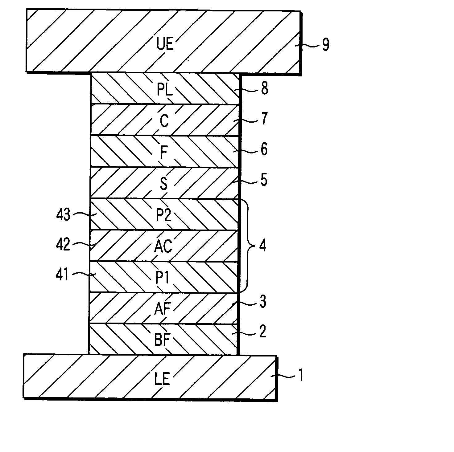
[0036]FIG. 1 is a sectional view of a magnetoresistive element according to the present Example. The magnetoresistive element (spin-valve) in FIG. 1 has a structure in which the following layers are stacked: a lower electrode (LE) 1, a buffer layer (BF) 2, an antiferromagnetic layer (AF) 3, a pinned layer 4 [a first pinned layer (P1) 41, an anti-parallel coupling layer (AC) 42, and a second pinned layer (P2) 43], a spacer layer (S) 5, a free layer (F) 6, a cap layer (C) 7, a protective layer (PL) 8, and an upper electrode (UE) 9. In the magnetoresistive element in FIG. 1, a sense current is supplied between the lower electrode 1 and upper electrode 9 in a direction substantially perpendicular to the thickness direction of the spin-valve the film, thus a CPP-GMR element is realized.

[0037] The magnetization of the first pinned layer 41 is substantially pinned in one direction by the antiferromagnetic layer 3, and the magnetization of the second pinned layer 43 is pinned, through the ...

example 2

[0051] In the present Example, a magnetoresistive element having the structure shown in FIG. 1 was fabricated using the materials listed below. [0052] Buffer layer 2: NiFeCr 4.1 nm, [0053] Antiferromagnetic layer 3: PtMn 15 nm, [0054] First pinned layer 41: Co90Fe10 3 nm, [0055] Anti-parallel coupling layer 42: Ru 1 nm, [0056] Second pinned layer 43: Co90Fe10 3 nm, [0057] Spacer layer 5: Cu 3 nm, [0058] Free layer 6: Co50Fe50 1 nm / Ni80Fe20 3.5 nm, with an fcc structure (stacked free layer), [0059] Cap layer 7: a material selected from Table 6, [0060] Protective layer 8: Ta 5 nm.

[0061] Table 6 shows materials used for the cap layer and the MR values of the CPP-GMR elements fabricated using the respective cap layers.

[0062] As seen in Table 6, compared to the CPP-GMR element without a cap layer, each CPP-GMR element having a cap layer on the free layer with the fcc structure exhibited an improved MR value in any case where the cap layer was formed of Cr (bcc structure) or Cr (bcc str...

example 3

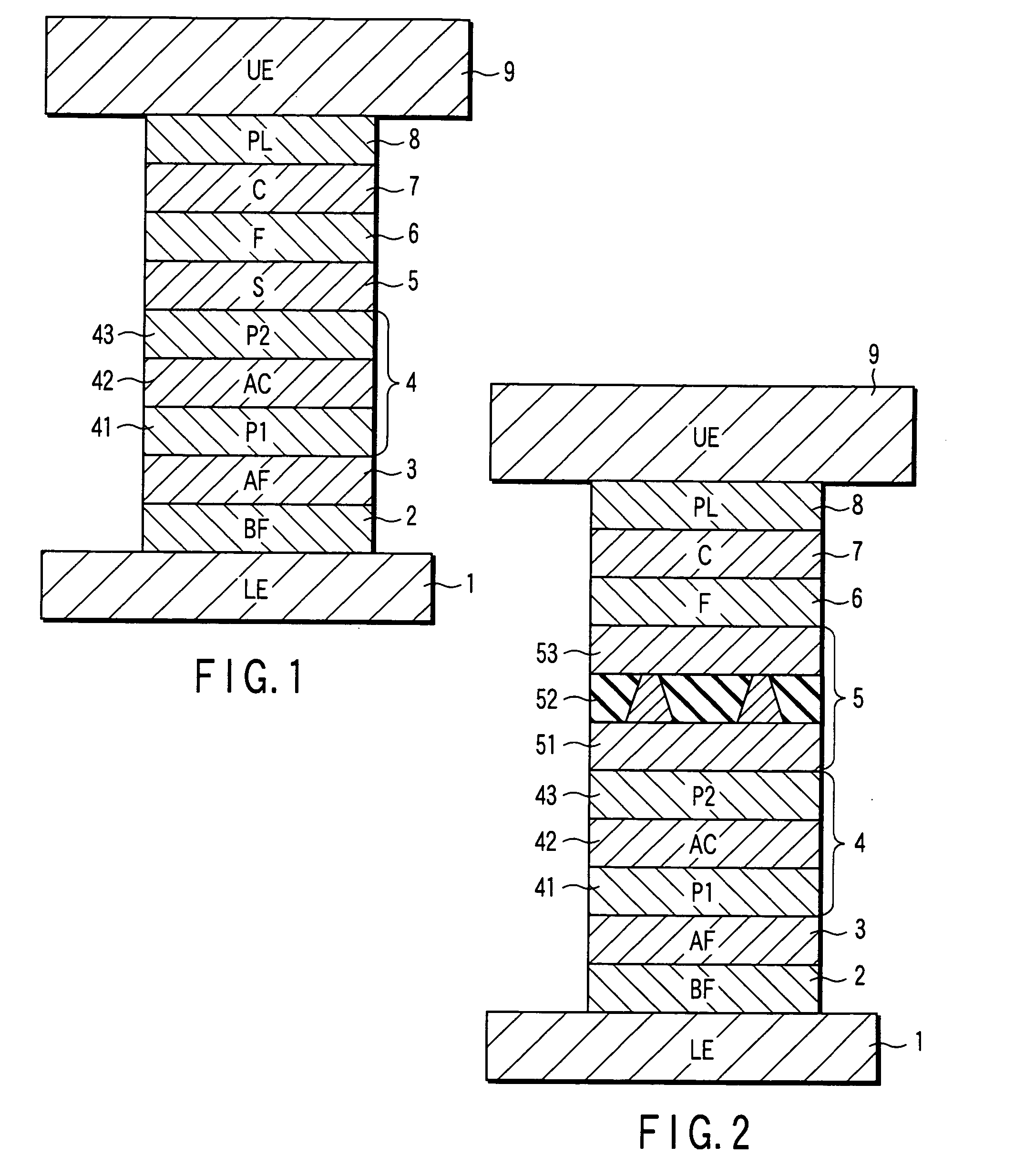
[0064]FIG. 2 is a sectional view of the magnetoresistive element according to the present Example.

[0065] The magnetoresistive element (spin-valve) in FIG. 2 has a structure in which the following layers are stacked: the lower electrode (LE) 1, the buffer layer (BF) 2, the antiferromagnetic layer (AF) 3, the pinned layer 4 [the first pinned layer (P1) 41, the anti-parallel coupling layer (AC) 42, and a second pinned layer (P2) 43], the spacer layer (S) 5 [the first metal layer 51, the resistance increasing layer 52, and the second metal layer 53], the free layer (F) 6, the cap layer (C) 7, the protective layer (PL) 8, and the upper electrode (UE) 9. The magnetoresistive element in FIG. 2 is different from one shown in FIG. 1 in that the spacer layer 5 has a structure in which the first metal layer 51, the resistance increasing layer 52, and the second metal layer 53 are stacked. The resistance increasing layer 52 includes an insulating layer and metal paths penetrating the insulatin...


PUM

PropertyMeasurementUnit
thicknessaaaaaaaaaa
thicknessaaaaaaaaaa
thicknessaaaaaaaaaa

Abstract

A magnetoresistive element has a magnetization pinned layer, a nonmagnetic spacer layer including a stack of a nonmagnetic metal layer, a resistance increasing layer and another nonmagnetic metal layer, a magnetization free layer having an fcc crystal structure, a cap layer having an fcc, an hcp, or a bcc crystal structure and having an interatomic distance between nearest neighbors greater than that of the magnetization free layer, and a pair of electrodes configured to provide a sense current in a direction substantially perpendicular to planes of the magnetization pinned layer, the nonmagnetic spacer layer, and the magnetization free layer.

Description

CROSS-REFERENCE TO RELATED APPLICATIONS [0001] This application is based upon and claims the benefit of priority from prior Japanese Patent Application No. 2004-069410, filed Mar. 11, 2004, the entire contents of which are incorporated herein by reference. BACKGROUND OF THE INVENTION [0002] 1. Field of the Invention [0003] The present invention relates to a magnetoresistive element, a magnetic head, and a magnetic recording and reproducing apparatus, and more specifically, to a magnetoresistive element configured to conduct a sense current in a direction perpendicular to a plane of a magnetoresistive film, as well as a magnetic head and a magnetic recording and reproducing apparatus using the magnetoresistive element. [0004] 2. Description of the Related Art [0005] In recent years, efforts have been made to reduce the sizes of magnetic recording media while increasing their capacities. Accordingly, the relative speed between a magnetic read head and a magnetic recording medium durin...

Claims


Application Information

Patent Timeline
Patent Type & Authority Applications(United States)
IPC IPC(8): G01R33/09G11B5/127G11B5/39G11B5/33H01F10/26H01F10/32H01L43/08
CPCB82Y10/00B82Y25/00G01R33/093G11B5/3906H01F41/325H01F10/3272H01L43/08H01F10/3259G11B2005/3996H10N50/10
Inventor FUKE, HIROMIFUKUZAWA, HIDEAKIYUASA, HIROMIHASHIMOTO, SUSUMUIWASAKI, HITOSHI
Owner KK TOSHIBA
Why Eureka
Try Eureka