

A kind of preparation method of four-junction solar cell based on gainnas material
A technology of solar cells and junction cells, applied in circuits, photovoltaic power generation, electrical components, etc., can solve the problems of crystal quality degradation, failure to obtain defective GaInNAs crystal layers, etc., to enhance lattice stability and reduce substrate transfer process , the effect of high crystal quality
- Summary
- Abstract
- Description
- Claims
- Application Information
AI Technical Summary
Problems solved by technology
Method used
Image

Examples
Embodiment Construction
[0037] In order to further understand the invention content, characteristics and effects of the present invention, the following examples are given hereby, but the embodiments of the present invention are not limited thereto, and the detailed description is as follows:
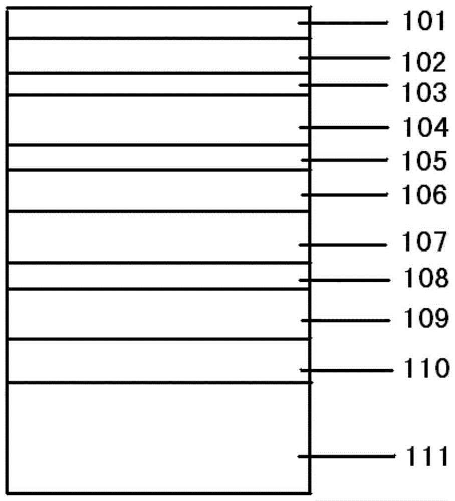
[0038] This embodiment is a preparation method of a four-junction solar cell based on GaInNAs material, comprising the following steps:
[0039] (1) providing a p-type Ge substrate;
[0040] The p-Ge substrate with [001] crystal orientation has a doping concentration of about 2×10 17 -5×10 17 cm -3 ; Ultrasonic removal of dirt particles on the surface of the GaAs substrate; washing with acetone and ethanol to remove surface organic matter; put the Ge substrate at 40-70 °C with a volume ratio of HF:H 2 o 2 :H 2 Etching in a mixed solution of O (1:8:1) for 1-2 minutes to remove surface oxides and organic matter; rinsing with deionized water; and drying the cleaned Ge substrate with filtered dry nitrogen. S...
PUM
 Abstract
Description
Claims
Application Information