Dynamic random access memory cell and method for fabricating the same

a random access memory and dynamic technology, applied in the direction of semiconductor devices, electrical equipment, transistors, etc., can solve the problems of complex manufacturing process, increasing the size of the memory device, etc., and achieve the effect of reducing the size of the dram cell

Active Publication Date: 2005-09-15
MARLIN SEMICON LTD
View PDF1 Cites 2 Cited by
  • Summary
  • Abstract
  • Description
  • Claims
  • Application Information

AI Technical Summary

Benefits of technology

[0008] An object of the present invention is to provide a DRAM cell and a method for fabricating the same to reduce the size of the DRAM cell.
[0009] Another object of the present invention is to provide a DRAM cell and a method for fabricating the same to simplify the manufacturing process and to reduce the costs.
[0018] The present invention provides a protruding electrode to cover the junction between the trench and the substrate and to serve a portion of the upper electrode. Hence, not only current leakage at the junction between the trench capacitor and the substrate is prevented, a higher capacitance coupling rate is provided. Further, because the present invention is compatible with the current logic process, manufacturing costs can be reduced, and the process can be simplified. Further, the present invention can be applied to the SOC. In addition, in accordance to the present invention, an electrode protruded from the trench, the capacitance is larger than the conventional capacitor.

Problems solved by technology

However, this also increases the size of the memory device.
How to increase the capacitance without increasing the size of the memory device is an important issue, especially when the integration level is getting higher and higher.
To form this structure, the manufacturing process is very complex.
Hence, how to simplify the structure and the manufacturing process of the DRAM cell is an important issue.
Ultimately, the size of the conventional deep trench capacitor cannot be reduced with the increase of the integration level.

Method used


Image

  • Dynamic random access memory cell and method for fabricating the same
  • Dynamic random access memory cell and method for fabricating the same
  • Dynamic random access memory cell and method for fabricating the same

Examples


Embodiment Construction

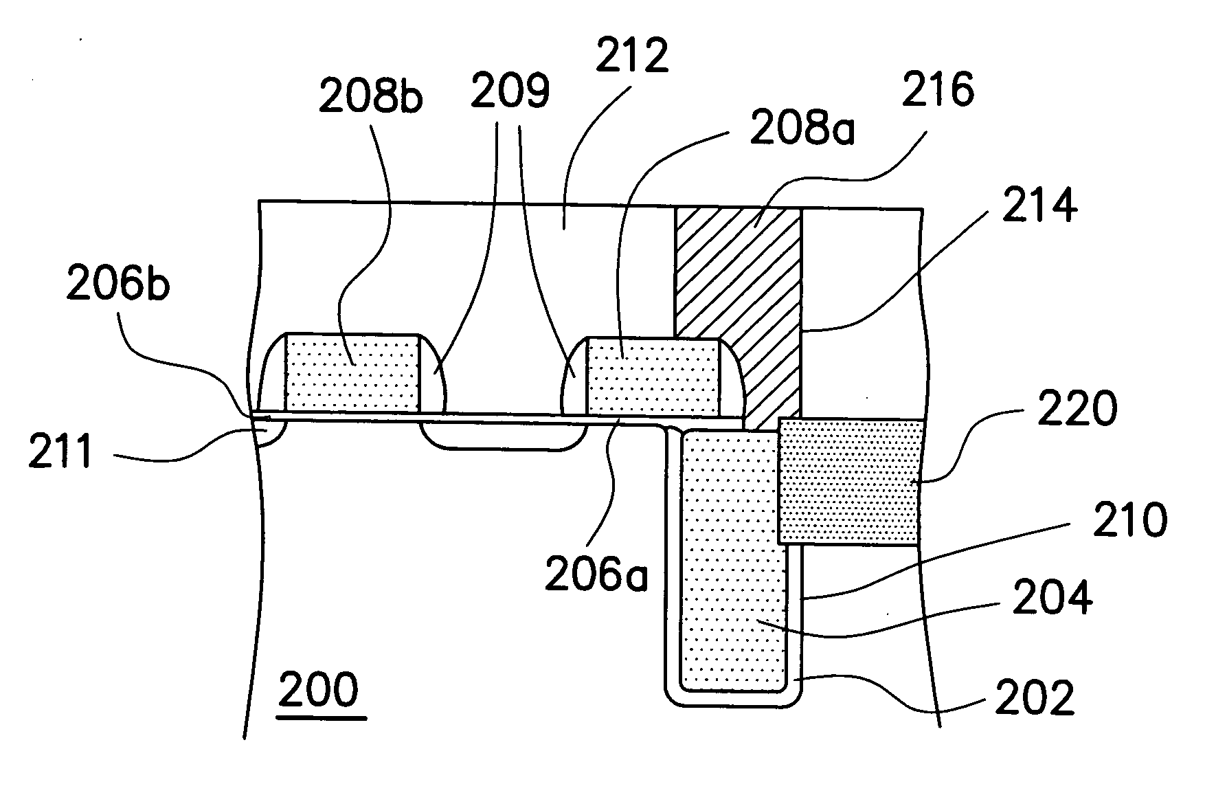
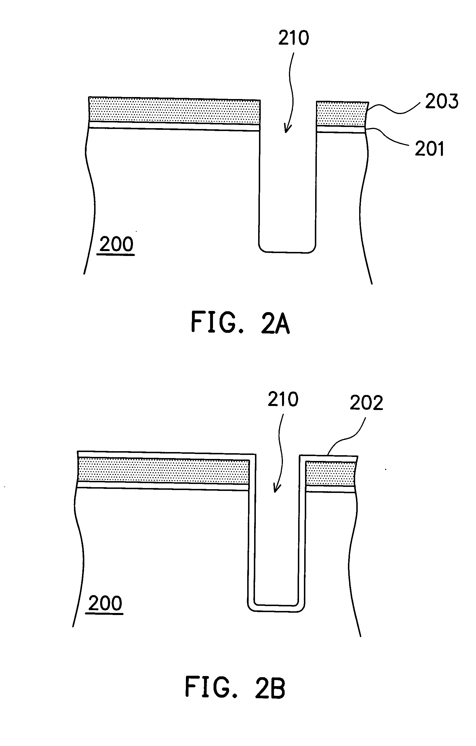
[0022]FIGS. 2A-2H are the cross-sectional views showing the steps of the fabrication process for a DRAM cell in accordance with a preferred embodiment of the present invention. The present invention can be applied to system-on-chip. Referring to FIG. 2A, a substrate 200 such as a silicon substrate is provided. A pad oxide layer 201 is formed on the substrate 200. Then, a mask layer 203 is formed on the pad oxide layer 201. Using the mask layer 230 as a mask, a trench 210 is formed by etching the substrate 200.

[0023] Referring to FIG. 2B, a capacitor dielectric layer 202 is formed on the substrate to cover the surface of the trench 210. The capacitor dielectric layer 202 can be a SiO2 / Si3N4 / SiO2 (ONO) stacked layer, or a Si3N4 / SiO2 (NO) stacked layer.

[0024] Referring to FIG. 2C, a first conducting layer 204 is formed in the trench 210. The material of the first conducting layer 204 is, for example, doped polysilicon. To form the first conducting layer 204 includes filling the trenc...


PUM

PropertyMeasurementUnit
electricallyaaaaaaaaaa
conductingaaaaaaaaaa
capacitanceaaaaaaaaaa

Abstract

A DRAM cell and a method for fabricating the same are provided. The method includes: forming a trench in a substrate; forming a first capacitor dielectric layer on the surface of the trench; forming a conducting layer inside the trench; forming a second capacitor dielectric layer on the surface of the substrate and on the conducting layer, wherein the substrate around the first and second capacitor dielectric layers serves as a bottom electrode; forming a protruding electrode on the substrate, the protruding electrode being on the substrate around the trench and covering a junction between the trench and the substrate; and electrically connecting the protruding electrode and the conducting layer, the conducting layer and the protruding electrode being an upper electrode.

Description

CROSS-REFERENCE TO RELATED APPLICATION [0001] This application claims the priority benefit of Taiwan application serial no. 92131757, filed on Nov. 13, 2003, the full disclosure of which is incorporated herein by reference. BACKGROUND OF THE INVENTION [0002] 1. Field of the Invention [0003] This invention generally relates to a method for fabricating a semiconductor device, and more particularly to a dynamic random access memory (DRAM) cell and a method fabricating the same. [0004] 2. Description of Related Art [0005] Capacitor plays an important role in storing data in a memory cell. The more charges the capacitor stores, lesser the noise will affect the reading / writing process for a memory cell. There are several ways to increase the capacitance such as increasing the surface area of the capacitor. However, this also increases the size of the memory device. How to increase the capacitance without increasing the size of the memory device is an important issue, especially when the i...

Claims


Application Information

Patent Timeline
Patent Type & Authority Applications(United States)
IPC IPC(8): H01L21/336H01L21/8242H01L27/108
CPCH01L27/10832H01L29/66181H01L27/10867H10B12/373H10B12/0385
Inventor LIN, YUNG-CHANGLIANG, CHIA-WENWANG, CHUAN-FU
Owner MARLIN SEMICON LTD
Why Eureka
Try Eureka