Semiconductor device and method of manufacturing the same

a semiconductor and semiconductor technology, applied in the field of semiconductor devices, can solve the problems of large device size, high cost, and high cost, and achieve the effects of low viscosity, high reliability of devices fabricated, and significant increase of adhesion strength

Inactive Publication Date: 2005-09-22
SANYO ELECTRIC CO LTD
View PDF10 Cites 29 Cited by
  • Summary
  • Abstract
  • Description
  • Claims
  • Application Information

AI Technical Summary

Benefits of technology

[0049] In the invention, the conductive foil to be a conductive pattern functions by itself as a supporting board, and the conductive foil supports the entire structure while the isolation trench is formed and while the circuit elements are mounted and covered with an insulating resin. When the conductive foil is separated into individual conductive patterns, the insulating resin functions as the supporting board. Accordingly, the minimum constitutive components—circuit element, conductive foil and insulating resin may be enough for the invention. This means that the invention does not require the supporting board that is indispensable in the related art technology of manufacturing circuit devices, and it reduces the production costs. In the invention, in addition, the supporting board is unnecessary, the conductive pattern is embedded in the insulating resin, and the thickness of the insulating resin and the conductive foil may be varied in any desired manner. Thus characterized by these advantages, still another advantage of the invention is that it produces extremely thin-walled circuit devices.
[0050] The manufacturing method of the invention is characterized by comprising a step of preparing conductive foil, and a step of forming a isolation trench that does not exceed the thickness of the conductive foil in a region thereof at least except the region to be a conductive pattern thereby to form the conductive pattern, and a step of coating at least a part of the surface of the conductive pattern with a thermosetting resin layer to fill the isolation trench, and a step of selectively removing the thermosetting resin layer in the site to which the electrodes of a circuit element mounted on the conductive pattern are bonded, and a step of fixing a circuit element above the conductive pattern and a step of forming a connecting means for electrically connecting the electrodes of the circuit element to the desired site of the conductive pattern, and a step of molding it with an insulating resin that covers the circuit element and bonds to the thermosetting resin layer.
[0051] In the manufacturing method of the invention, since the conductive pattern is coated with a semi-cured thermosetting resin layer immediately after its formation, the isolation trench can be completely filled with a liquid thermosetting resin of low viscosity, and the adhesion strength of the two is significantly increased. In addition, since the thermosetting resin layer covers the conductive pattern immediately after the conductive pattern has been formed, the surface of the conductive pattern is not oxidized in the subsequent heating step for die bonding or wire bonding, and the reliability of the devices fabricated is high.

Problems solved by technology

However, the package-type semiconductor device 501 does not satisfy the requirements of down-sizing, thickness reduction and weight reduction, since the lead terminal 504 is led outside from the resin layer 503 and since the overall size of the device is large.
However, the ceramic substrate used herein is extremely brittle and is readily cracked, different from flexible sheets and glass-epoxy substrates, and is therefore problematic in that it is not applicable to resin mold sealing.
However in case of adopting a flexible sheet 50 as an interposer board, the flexible sheet formed on a rear surface of IC chip is very expensive, and there are problems that cost rises, thickness of the package becomes thick, and weight increases.
There is a problem that heat resistance from a back face of the IC chip to a back face of the package becomes large in a supporting board because the supporting board comprises material other than metal.
Therefore there is a problem that driving current does not flow fully because of temperature rise of IC chip at driving.
Heretofore, It has heretofore been difficult to provide a down-sized, thin-walled and lightweight circuit device that comprises these constitutive elements.
For these reasons, the glass-epoxy substrate 505 is indispensably used and it increases the production costs.
In addition, since the glass-epoxy substrate 505 is thick, the circuit device comprising it is inevitably thick and is limited in point of down-sizing, thickness reduction and weight reduction.
Further, the glass-epoxy substrate and the ceramic substrate indispensably require a step of forming through-holes through which the electrodes formed on the two surfaces thereof are connected to each other, and therefore manufacturing time is long and industrial-scale mass production is very difficult.

Method used


Image

  • Semiconductor device and method of manufacturing the same
  • Semiconductor device and method of manufacturing the same
  • Semiconductor device and method of manufacturing the same

Examples


first embodiment

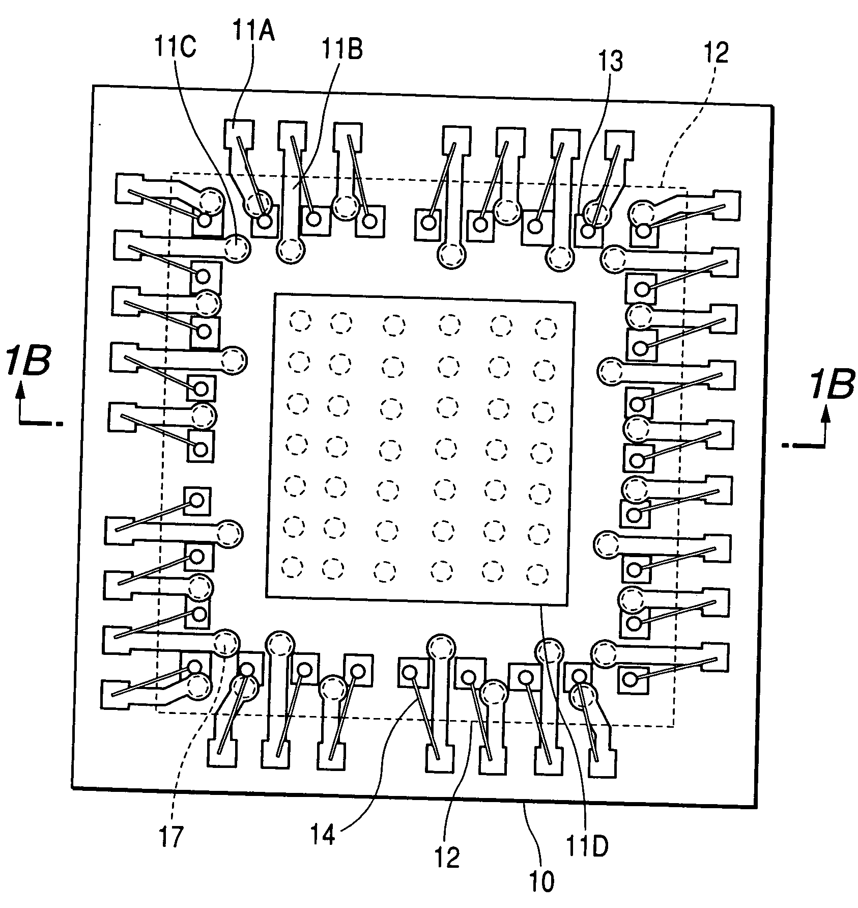
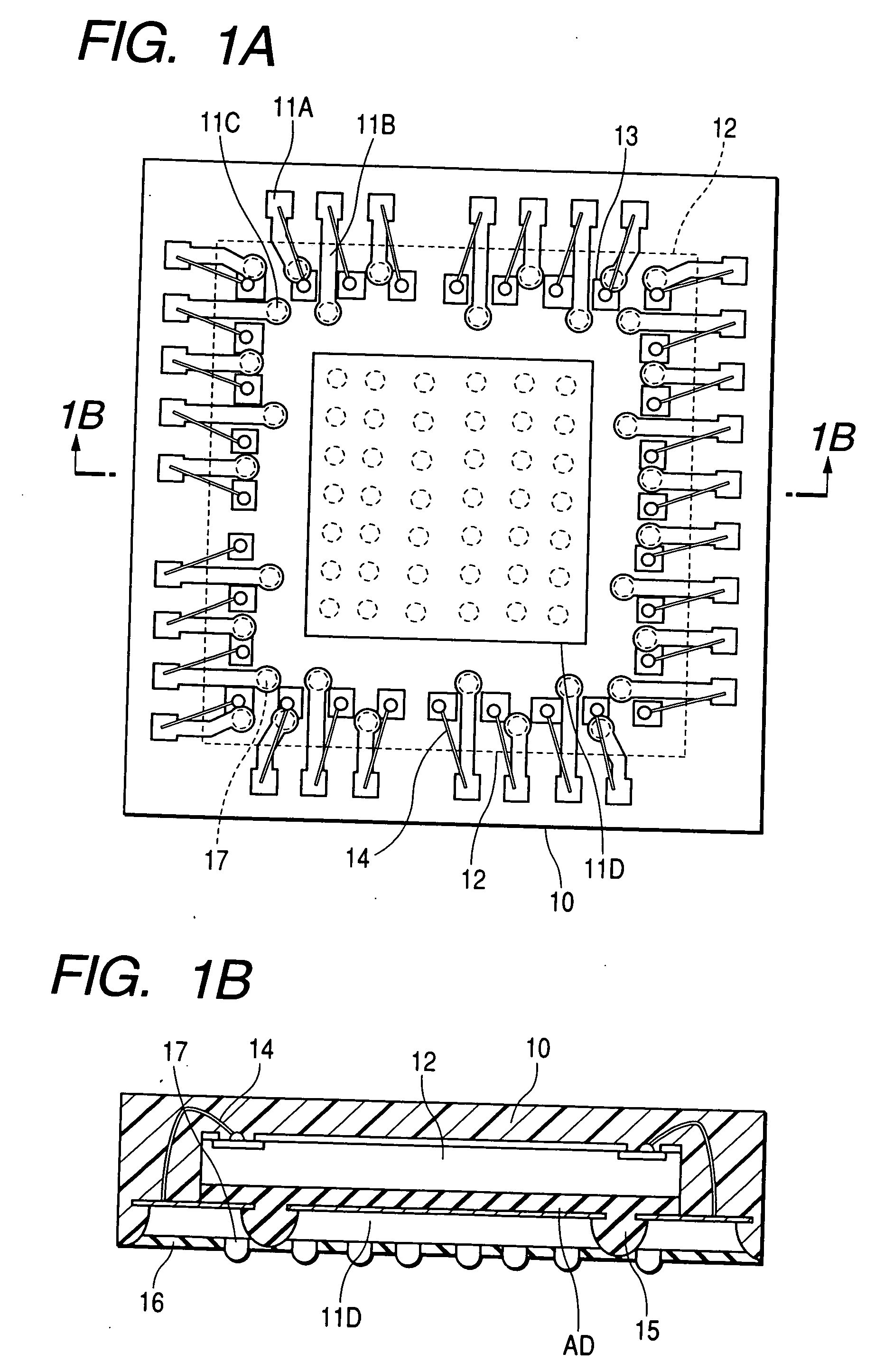
[0103] First, a semiconductor device of the invention is described referring to FIG. 1. FIG. 1A is a plan view of the semiconductor device, and FIG. 1B is a section view cut with A-A line.

[0104]FIG. 1 shows a insulating resin 10 buried with the following chips. They are pads 11A, conductive paths 11B in one-body with the pads 11A, external connection electrodes 11C provided at the other ends of the conductive paths 11B in one body with the conductive paths 11B. Further an electrode for radiating 11D provided at one area surrounded by the conductive patterns 11A, 11B, and 11C and a semiconductor chip 12 provided on the electrode for radiating 11D are buried. The semiconductor chip 12 is fixed to the electrode for radiating 11D through a insulating adhesion means AD, and is shown with dotted line in FIG. 1A.

[0105] A bonding electrode 13 of the semiconductor chip 12 and the pad 11A are electrically connected through a bonding wire 14.

[0106] Side face of said conductive pattern 11A t...

second embodiment

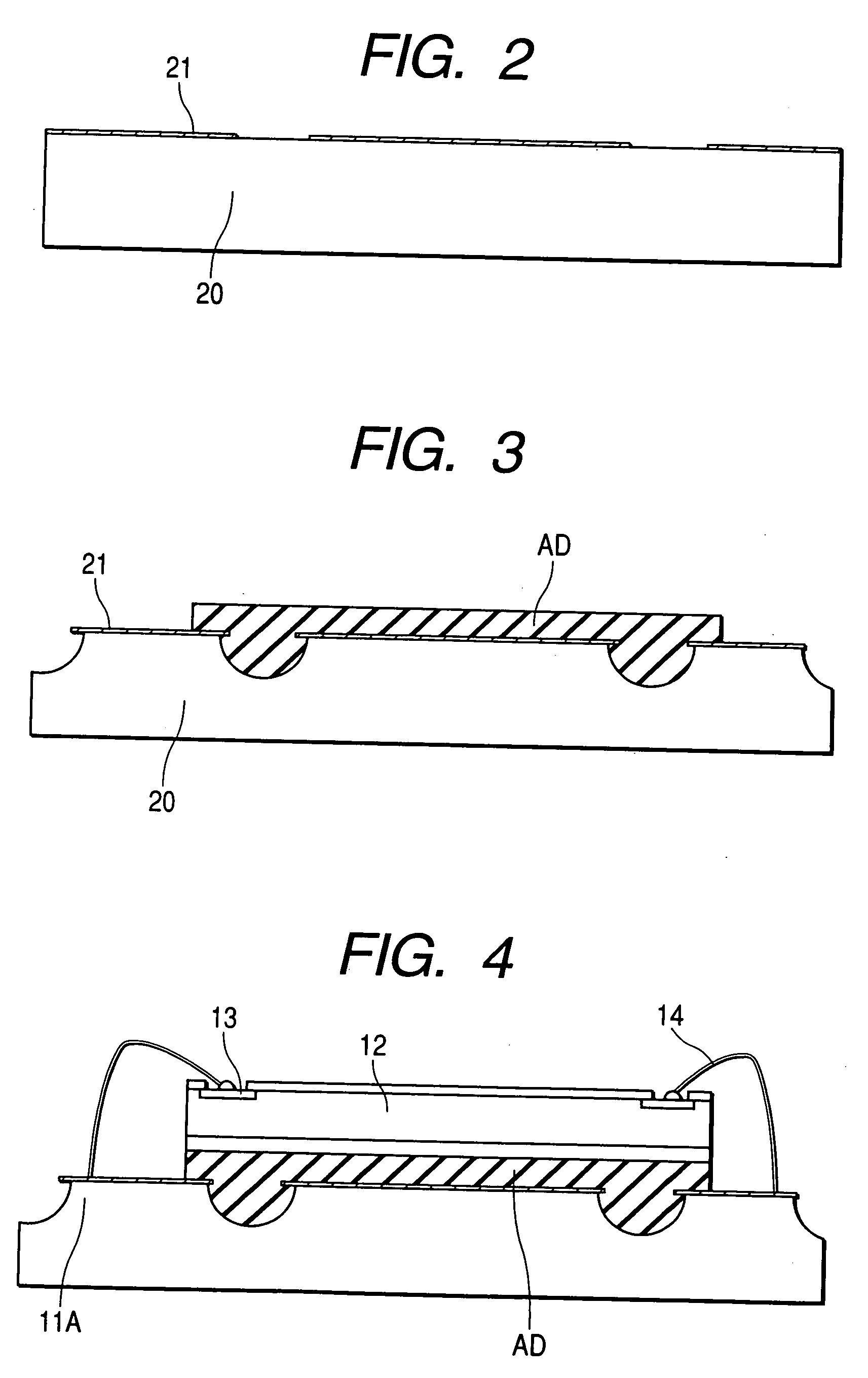
[0115] The method for manufacturing shows the method for manufacturing of the semiconductor chip 15 shown in FIG. 1, and FIG. 2 to FIG. 6 are section views corresponding to A-A line of FIG. 1A.

[0116] First, a conductive foil 20 is provided as FIG. 2. Thickness thereof is desirably 10 μm to 300 μm, here rolled copper foil of 70 μm is used. Next on the front face of the conductive foil 20, a conductive film 21 or a photo resist is formed as etching-resist.

[0117] The pattern is same pattern as the pads 11A in FIG. 11A, the conductive paths 11B, the external connection electrode 11C, and the electrodes for radiation 11D. In the case of using the photo resist instead of the conductive film 21, a conductive film such as Au, Ag, Pd or Ni is formed at a part corresponding to at least pad in the lower layer of the photo resist. This is provided to make bonding possible. (Refer FIG. 2 about the above.)

[0118] Next, a conductive foil 20 is half-etched through said conductive film 21 or photo...

third embodiment

[0146]FIG. 8 shows the semiconductor device 42. FIG. 8A is a plan view of the device, and FIG. 8B is a section view cut by A-A line.

[0147] Although the pad 11A is formed in one body with the conductive path 11B and the external connection electrode 11C in FIG. 1, here the back face of the pad 11A becomes the external connection electrode.

[0148] As the back face of the pad 11A is formed in rectangle, the pattern exposing from the insulating film 16 is formed in same pattern as said rectangle. The trenches 43 are formed so that the electrode 11D for radiation and chip 12 can be adhered appropriately by filling the insulating adhesion means into said trenches. Thereby the electrode 11D for radiation is divided to plural.

[0149] As clear from the above description, in the invention, even the conductive foil (or conductive foil) where the conductive pattern formed in island shape has thickness is buried in the insulating adhesion means and the insulating resin. As the electrode for rad...


PUM


Abstract

As conductive patterns 11A to 11D are formed burying in a insulating resin 10 and a conductive foil 20 is formed being half-etched, thickness of the device is made thin. As an electrode for radiation 11D is provided, a semiconductor device superior in radiation is provided.

Description

BACKGROUND OF THE INVENTION [0001] 1. Description of the Related Art [0002] The present invention relates to a semiconductor device and a method for manufacturing the same, particularly a semiconductor device radiating excellently heat from the semiconductor device and a method for manufacturing the same. [0003] 2. Description of the Related Art [0004] In recent years, use of IC package for portable equipment or small, hi-density mounting equipment progresses, and the conventional IC package and its concept of mounting are largely changing. These details are described in CSP technology, and mounting material and device supporting the technology—special issue of DENSHI ZAIRYO (p. 22, September 1998). [0005]FIG. 9 is a structure adopting a flexible sheet 50 as an interposer board, a copper foil pattern 51 is put on the flexible sheet through adhesive, and an IC chip is fixed. There is a pad for bonding 53 formed at periphery of the IC chip as the conductive pattern 51. A pad for conne...

Claims


Application Information

Patent Timeline
Patent Type & Authority Applications(United States)
IPC IPC(8): H01L21/48H01L23/31H01L23/48H01L23/495
CPCH01L21/4828H01L21/4832H01L23/3107H01L23/3121H01L23/3128H01L23/49513H01L24/32H01L24/48H01L24/97H01L2221/68377H01L2224/05639H01L2224/05644H01L2224/05655H01L2224/05664H01L2224/32225H01L2224/32245H01L2224/45144H01L2224/48091H01L2224/48227H01L2224/48228H01L2224/48247H01L2224/48465H01L2224/73265H01L2224/83855H01L2224/83856H01L2224/85447H01L2224/97H01L2924/01005H01L2924/01006H01L2924/01011H01L2924/01013H01L2924/01014H01L2924/01015H01L2924/01028H01L2924/01029H01L2924/01046H01L2924/01047H01L2924/01059H01L2924/01078H01L2924/01079H01L2924/01082H01L2924/014H01L2924/14H01L2924/15311H01L2924/19041H01L2924/19043H01L2924/19105H01L2224/83385H01L24/45H01L2924/01024H01L2924/01033H01L2924/0132H01L2924/12041H01L2224/48644H01L2224/48655H01L2224/48664H01L2224/48639H01L2924/07802H01L2924/00014H01L2224/85H01L2224/83H01L2224/92247H01L2924/00H01L2924/01026H01L2924/00012H01L24/49H01L24/73H01L2224/05554H01L2224/48647H01L2224/49171H01L2924/12042H01L2924/15787H01L2924/181H01L2924/351
Inventor SAKAMOTO, NORIAKIKOBAYASHI, YOSHIYUKISAKAMOTO, JUNJIOKADA, YUKIOIGARASHI, YUSUKEMAEHARA, EIJUTAKAHASHI, KOUJINAKAMURA, TAKESHI
Owner SANYO ELECTRIC CO LTD
Why Eureka
Try Eureka