High thickness uniformity vaporization source

a vaporization source and uniformity technology, applied in vacuum evaporation coating, mechanical equipment, machines/engines, etc., can solve the problems of increasing the intensity of emitted light, low deposition rate on the substrate, and insufficient oled devices, so as to reduce the heat radiated toward the substrate, reduce the deposition uniformity of vaporized organic materials, and minimize material degradation

Active Publication Date: 2005-09-22
GLOBAL OLED TECH
View PDF11 Cites 22 Cited by
  • Summary
  • Abstract
  • Description
  • Claims
  • Application Information

AI Technical Summary

Benefits of technology

[0015] It is an advantage of the present invention that it increases the deposition uniformity of vaporized organic material while reducing the heat radiated toward a substrate. It is a further advantage that only a small portion of organic material is exposed to vaporization temperatures at a given time, thereby minimizing material degradation. By operating at a reduced throw distance, the material utilization is improved as well as the apparent deposition rate. More of the organic material is deposited on the substrate and less on the walls of the vacuum chamber.

Problems solved by technology

This has been adequate for early OLED devices but is not adequate for OLED devices that rely on the organic layer stack thickness to act as a resonance cavity and thereby increase the intensity of the emitted light.
This strategy requires large deposition chambers, results in very low deposition rates on the substrate and wastes the vast majority of sublimated organic material.
Perhaps more problematic to the substrate, the organic film, and any masks used to define pixels, is the increased heat radiated from the source to the substrate at short throw distances.
The increased heating alters the organic film nucleation process and dilates the substrate and mask, making it impossible to maintain precise alignment.

Method used


Image

  • High thickness uniformity vaporization source
  • High thickness uniformity vaporization source
  • High thickness uniformity vaporization source

Examples


Embodiment Construction

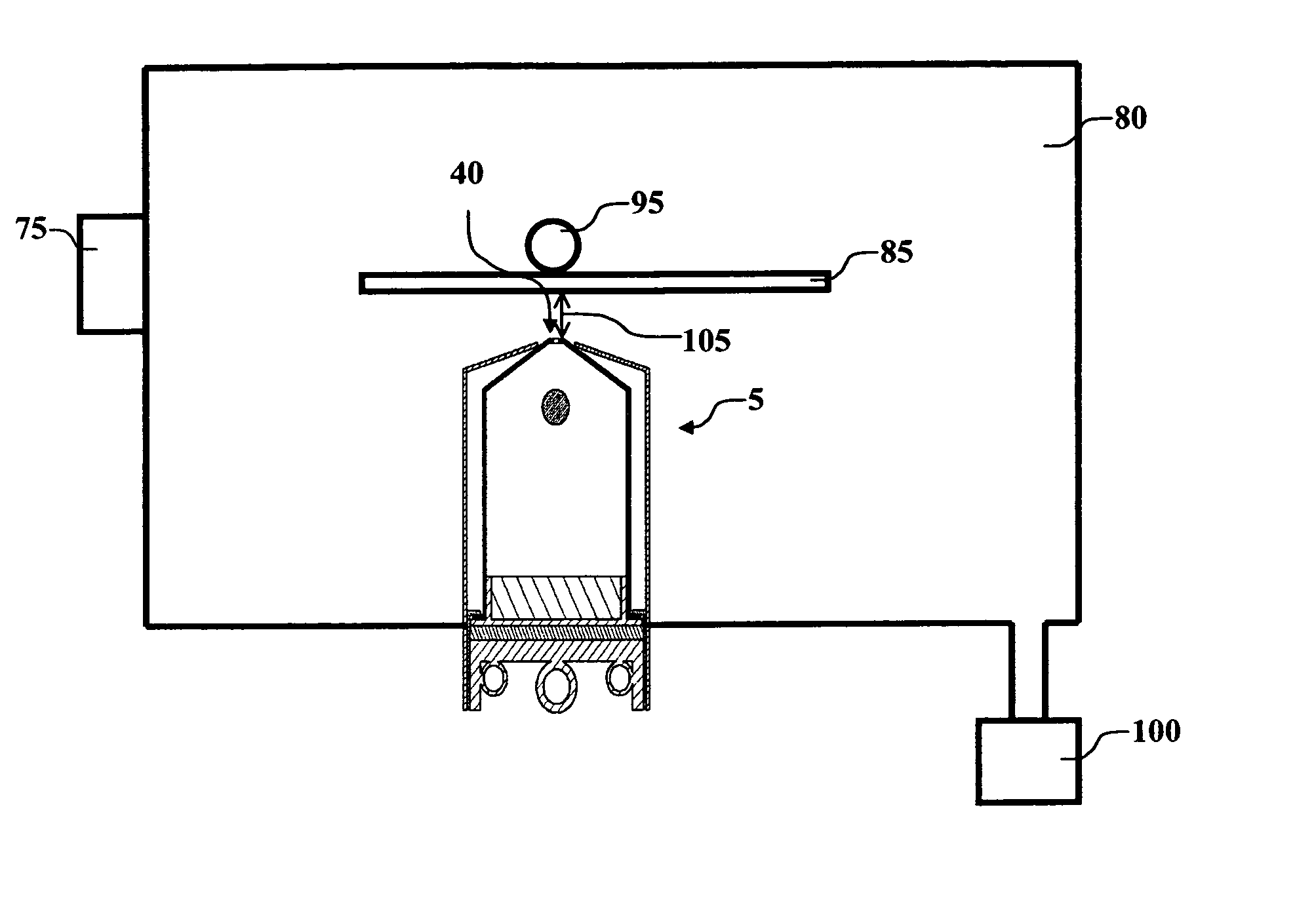
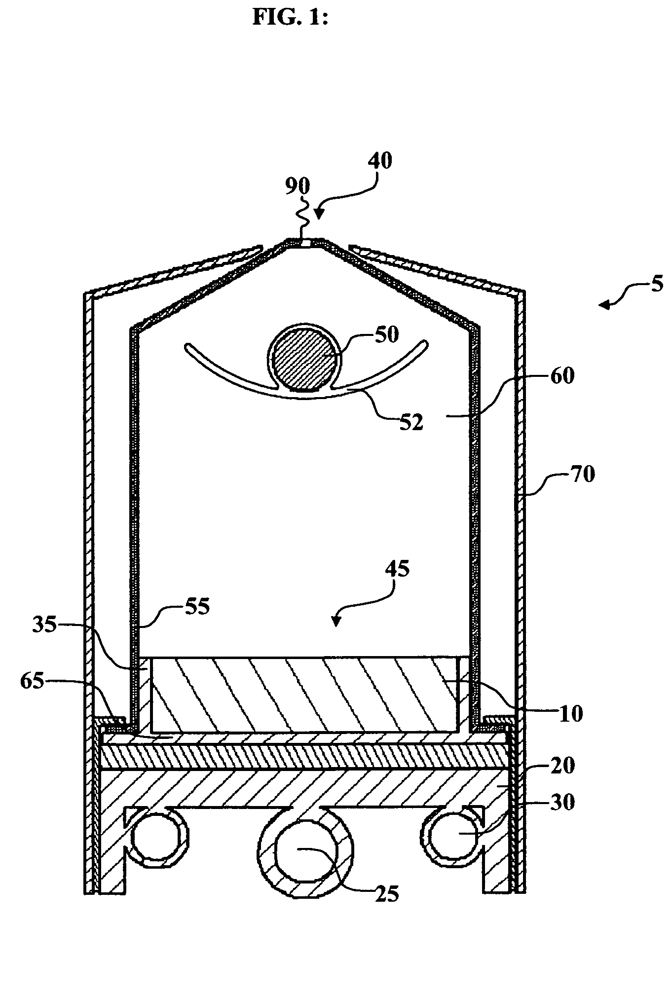
[0024] Turning now to FIG. 1, there is shown a cross-sectional view of one embodiment of a device according to the present invention. Vapor deposition source 5 is a device for vaporizing organic materials and thereby coating an organic layer onto a substrate surface of an OLED device to form a film. Vapor deposition source 5 includes manifold 60, which is an enclosed volume for containing vaporized organic material. Manifold 60 is bounded by aperture plate 40, side walls 55 and bottom wall 65. Side walls 55 are understood to include any necessary end walls to make manifold 60 completely enclosed. Side walls 55 and bottom wall 65 define chamber 45 for receiving organic material 10. The upper portion of manifold 60 engages the lower portion through a seal area 35. The seal can take the form of a labyrinth seal, a face seal or an O-ring seal. It is not necessary for the seal to initially be gas tight, since, due to the relatively low temperature in the seal area, escaping vapors will q...


PUM

PropertyMeasurementUnit
emissivityaaaaaaaaaa
pressureaaaaaaaaaa
work functionaaaaaaaaaa

Abstract

A vapor deposition source for use in vacuum chamber for coating an organic layer on a substrate of an OLED device, includes a manifold including side and bottom walls defining a chamber for receiving organic material, and an aperture plate disposed between the side walls, the aperture plate having a plurality of spaced apart apertures for emitting vaporized organic material; the aperture plate including conductive material which in response to an electrical current produces heat; means for heating the organic material to a temperature which causes its vaporization, and heating the side walls of the manifold; and an electrical insulator coupling the aperture plate to the side walls for concentrating heat in the unsupported region of the aperture plate adjacent to the apertures, whereby the distance between the aperture plate and the substrate can be reduced to provide high coating thickness uniformity on the substrate.

Description

CROSS REFERENCE TO RELATED APPLICATIONS [0001] Reference is made to commonly assigned U.S. patent application Ser. No. 10 / 352,558 filed Jan. 28, 2003 by Jeremy M. Grace et al., entitled “Method of Designing a Thermal Physical Vapor Deposition System”, U.S. patent application Ser. No. 10 / 784,585 filed Feb. 23, 2004, by Michael Long et al, entitled “Device and Method for Vaporizing Temperature Sensitive Materials”, U.S. patent application Ser. No. ______ filed concurrently herewith, by Michael Long et al, entitled “Vaporizing Fluidized Organic Materials”, the disclosures of which are herein incorporated by reference.FIELD OF THE INVENTION [0002] The present invention relates to the field of physical vapor deposition where a source material is heated to a temperature so as to cause vaporization and create a vapor plume to form a thin film on a surface of a substrate. BACKGROUND OF THE INVENTION [0003] An organic light emitting device (OLED) includes a substrate, an anode, a hole-transp...

Claims


Application Information

Patent Timeline
Patent Type & Authority Applications(United States)
IPC IPC(8): C23C14/12C23C14/24C23C14/26
CPCC23C14/12C23C14/26C23C14/243C23C14/24
Inventor LONG, MICHAELGRACE, JEREMY M.KOPPE, BRUCE E.FREEMAN, DENNIS R.REDDEN, NEIL P.ZWAAP, ROBERT F.
Owner GLOBAL OLED TECH
Why Eureka
Try Eureka