Electronic device and methods for fabricating an electronic device

a technology of electronic devices and electrodes, applied in semiconductor devices, solid-state devices, transistors, etc., can solve the problems of increasing the time needed to place charge on the pixel electrodes, limited use of organic semiconductors in tfts in backplanes for displays, and devices with staggered geometries can have larger output currents

Active Publication Date: 2005-09-22
XEROX CORP
View PDF6 Cites 3 Cited by
  • Summary
  • Abstract
  • Description
  • Claims
  • Application Information

AI Technical Summary

Benefits of technology

[0009] The use of organic semiconductors can have advantages over amorphous silicon, especially for flexible electronics. Organic semiconductors are sometimes processed using low-cost techniques, are sometimes deposited at the low temperatures (e.g., lower than 150° C.) required for plastic substrates, and tolerate mechanical stress. The development of micron-scale processing techniques for organic semiconductors is also beneficial.
[0010] The use of organic semiconductors in TFTs in backplanes for displays is limited by their lower field effect mobility relative to amorphous silicon semiconductors. A TFT in a pixel element in a backplane provides current to place charge on a pixel electrode that causes a change in the display at that pixel. The existence of injection barriers at the contacts of organic TFTs can limit the maximum possible output current of the device and thus increases the time needed to place charge on the pixel electrode. In order to solve this problem, and to achieve the current required to charge a pixel electrode in a typical display, the electronic device, such as, for example, the transistor, is enlarged. This enlargement decreases the fill factor of the pixel in the display because of the increase in spatial area of the TFT in the pixel element.
[0011] The output current of the some organic electronic devices, such as, a thin film transistor, depends on the geometry of the device due to the presence of injection barriers at the source and drain contacts. Devices with staggered geometries can have larger output currents than devices with coplanar geometries due to decreased contact resistances. However, the manufacturing of devices with coplanar geometries is easier than the manufacturing of devices with staggered geometries, and is preferred for display applications.
[0014] Various separable exemplary embodiments of the devices and methods according to this invention have one staggered contact. This allows for a larger output current without necessarily enlarging the TFT. Thus, the quality of the image on the display experiences reduced degradation.

Problems solved by technology

The use of organic semiconductors in TFTs in backplanes for displays is limited by their lower field effect mobility relative to amorphous silicon semiconductors.
The existence of injection barriers at the contacts of organic TFTs can limit the maximum possible output current of the device and thus increases the time needed to place charge on the pixel electrode.
Devices with staggered geometries can have larger output currents than devices with coplanar geometries due to decreased contact resistances.
Another problem commonly associated with organic devices such as, for example, transistors, is the type of material used as a via layer.
These processing steps can damage the organic semiconductor.

Method used


Image

  • Electronic device and methods for fabricating an electronic device
  • Electronic device and methods for fabricating an electronic device
  • Electronic device and methods for fabricating an electronic device

Examples


Embodiment Construction

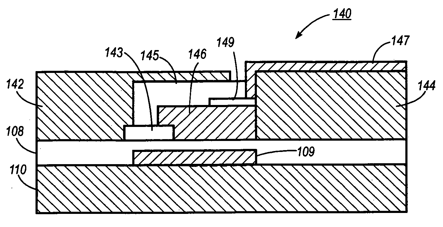
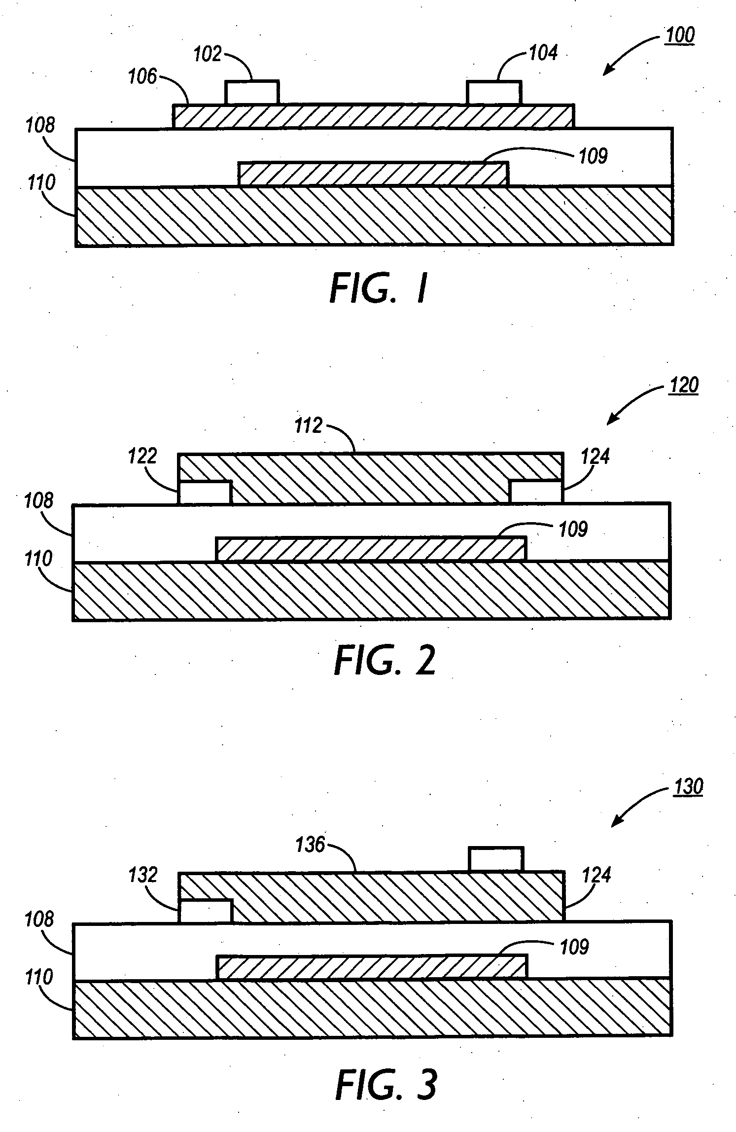
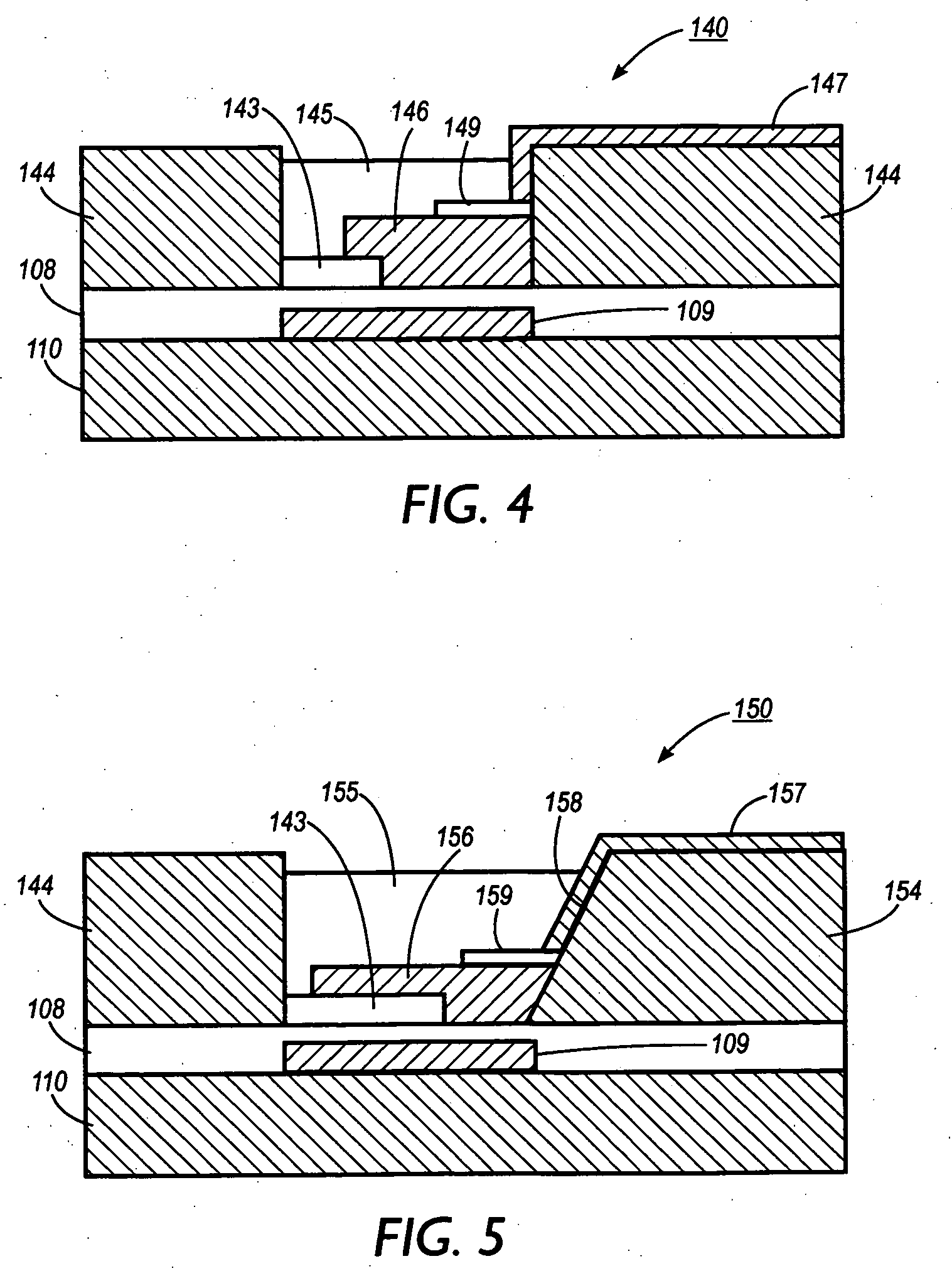
[0038]FIGS. 1-3 show illustrations of electronic devices 100, 120 and 130. A dielectric layer 108 is formed over a substrate 110 and over a gate electrode 109, and a semiconductor 106 is formed over the dielectric layer 108. In FIG. 1, an electrode 102 and an electrode 104 are located over the semiconductor 106. In FIG. 2, an electrode 122 and an electrode 124 are located between the semiconductor 112 and the substrate 110. In FIG. 3, an electrode 132 is located between the semiconductor 136 and the gate electrode 110, and an electrode 134 is located over the semiconductor 136. When electrode 102 and the electrode 104 are located over the semiconductor 106, such as in FIG. 1, for example, the electronic device 100 is said to be in a staggered configuration. When the electrode 122 and the electrode 124 are located between the semiconductor 112 and the gate electrode 110, as in FIG. 2, for example, the electronic device 120 is said to have a coplanar configuration. When the electrode ...


PUM

PropertyMeasurementUnit
temperaturesaaaaaaaaaa
areaaaaaaaaaaa
chargeaaaaaaaaaa

Abstract

An electronic device and a method of fabricating the electronic device includes forming a first electrical contact, a dielectric layer and a second electrical contact wherein the dielectric layer is located between the first and the second electrical contacts, forming an electrically insulating layer over the dielectric layer and the first electrical contact, exposing the first and second electrical contact, the dielectric layer and a first portion of the electrically insulating layer to radiation from the side of the first electrical contact, removing a second portion of the electrically insulating layer that was not irradiated by the radiation, providing a semiconductor material over a portion of the dielectric layer, and forming at least a third electrical contact over at least a portion of the electrically insulting layer and the semiconductor material.

Description

BACKGROUND OF THE INVENTION [0001] This is a Division of application Ser. No. 10 / 739,189 filed Dec. 19, 2003. The entire disclosure of the prior application is hereby incorporated by reference herein in its entirety. [0002] 1. Field of Invention [0003] This invention relates to electronic devices such as, for example, transistors and methods for fabricating the same. [0004] 2. Description of Related Art [0005] Electronic devices, such as, for example, transistors, have a multitude of uses. For example, low cost, large area arrays of thin-film transistors (TFTs) are important components in flat panel displays, electric paper, and imagers. In a pixel of a display, a TFT is used as an electrical switch to charge a pixel electrode that switches the display media from one state to another. A display backplane comprises an array of pixel elements that is used to address the display media. Amorphous silicon is often used as the active material in TFTs for these applications. [0006] Polymer...

Claims


Application Information

Patent Timeline
Patent Type & Authority Applications(United States)
IPC IPC(8): H01L21/00H01L21/336H01L21/28H01L29/41H01L29/417H01L29/76H01L29/786H01L51/05H01L51/40
CPCH01L29/41733H01L51/057H01L51/0545H01L51/0021H10K71/60H10K10/466H10K10/491
Inventor CHABINYC, MICHAEL L.SALLEO, ALBERTOWONG, WILLIAM S.
Owner XEROX CORP
Why Eureka
Try Eureka