Photovoltaic module package

Active Publication Date: 2014-06-12
CORNING INC
View PDF14 Cites 28 Cited by
  • Summary
  • Abstract
  • Description
  • Claims
  • Application Information

AI Technical Summary

Benefits of technology

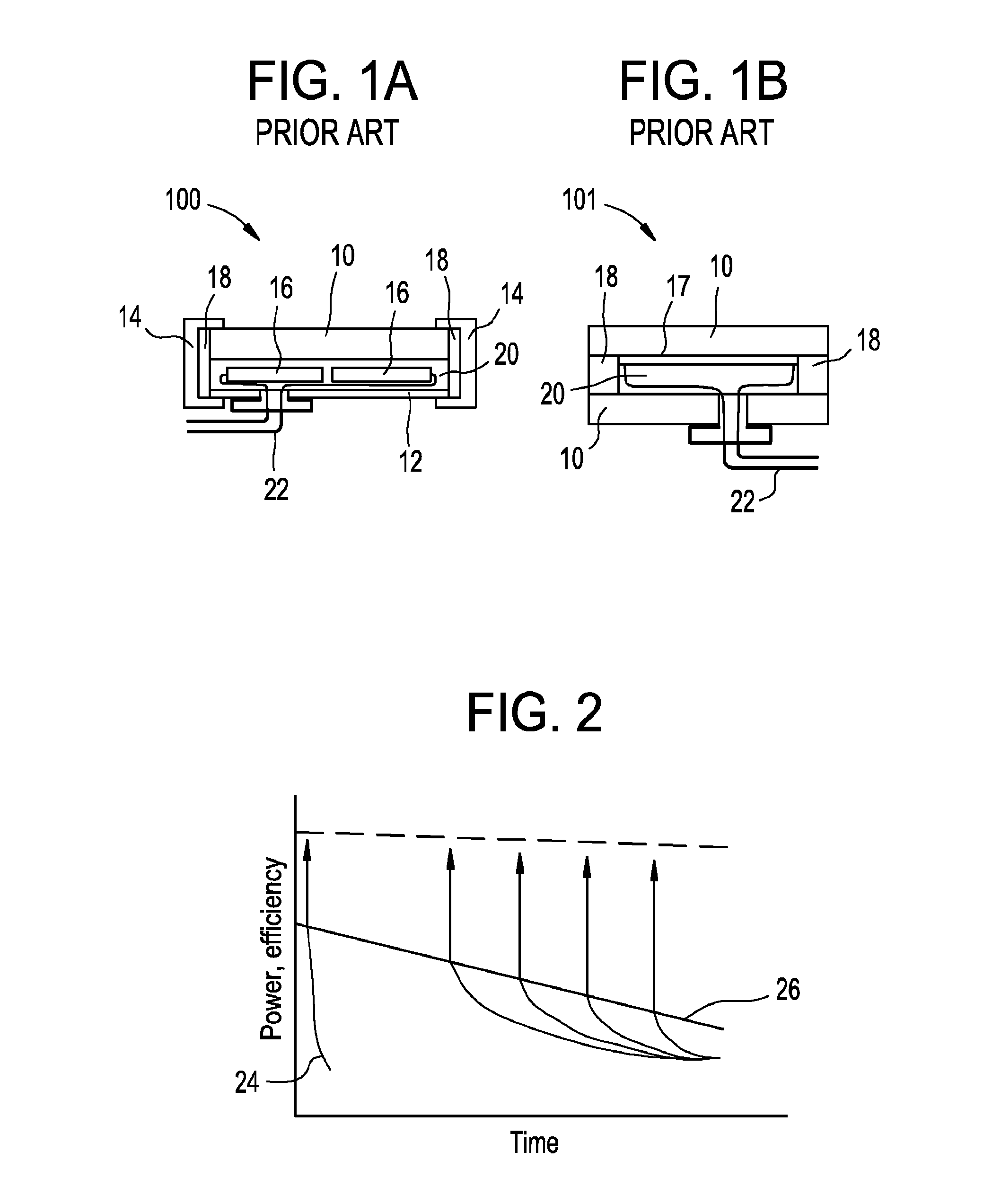
[0007]It is desirable to have high initial conversion efficiencies and low degradation rates over the module life to increase the amount of electricity produced and decrease the levelized cost of electricity (LCOE) or $/kilowatt hour produced. FIG. 2 illustrates the improvements in these two areas. Improvement of initial module efficiencies shown by line 24 can be generated by improvement of cell performance. Other ways of improving the initial module performance include maximizing the cell aperture for a given module size. The edge delete regions and the area c

Problems solved by technology

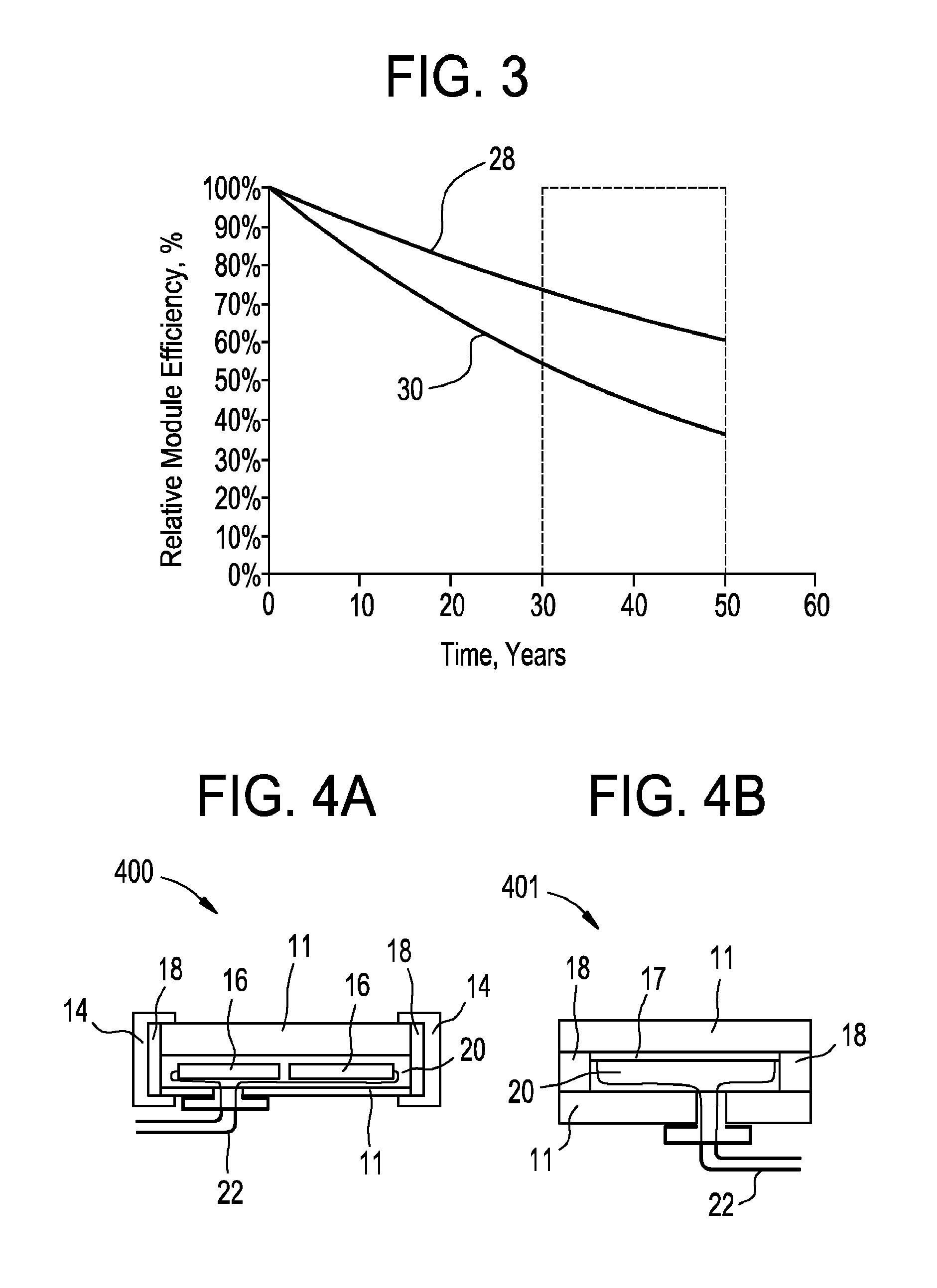
Wafered and thin-film photovoltaic modules both exhibit a continuous degradation in performance over their lifetimes, with thin-film modules degrading more quickly.
This degradation can be linked to a multitude of issues

Method used


Image

  • Photovoltaic module package
  • Photovoltaic module package
  • Photovoltaic module package

Examples


Example

Example 1

[0122]Conduction of electrical charge in glass is primarily due to ions in response to an applied voltage. The volume conductivity (which is the inverse of the resistivity) of glass as shown in FIG. 11 is obtained using established sample preparation protocols and measurement techniques. The glass samples under test are prepared as described in ASTM D257, where flat samples are finished to a defined area and thickness before gold electrodes are fired on opposite flat surfaces to form a parallel-plate capacitor. Electrical connections are then made to the sample and placed in a furnace as described by ASTM C657. The impedance of the parallel-plate electrode sample is measured using an impedance spectrum analyzer and the conductivity is calculated using the following two descriptions for resisitivity ρ (Ω·cm): (1) ρ=R·(A / t), where R=is the resistance (Ω) and A and t are the effective area and thickness of the sample, respectively; and (2) ρ=ρ0·e(−EA / kBT) where ρ0 is the pre-e...

Example

Example 2

[0123]The Wet leakage test is performed at +600 V and stabilized for 2 minutes per the IEC 61215 measurement guidelines. The minimum measurement requirement for modules is 40 Mohm*m2.

TABLE 1MΩ· m2MaxMinAvgSLG front sheet / 109.8982.1488.12polymer back sheetComp. 106 / 10674740.007437.0034332.64

Wherein “SLG” is a standard soda lime glass front sheet and the back sheet comprised a Tedlar polymer. From our measurements, a soda lime glass (SLG) / polymer package passes the IEC requirement. The embodied PV module package comprises front and back sheet glass sheet compositions of composition 106 (TABLE 3). The embodied PV module package passes with >3 orders of magnitude better margin in performance. The higher resistance from the embodied PV package is in part attributed to the >3 orders of magnitude higher resistivity of the 106 glass versus SLG.

Example

Example 3

[0124]Potential induced degradation (“PID”) is tested via the Damp-heat test on a number of photovoltaic modules to compare the reliability, performance, and stability of the embodiments. Standard c-Si module design is used, with all devices comprising components from either Construction 1 or Construction 2 (See TABLE 4). The modules all comprise c-Si cells, encapsulant coating, front and back sheet components, a framing gasket, an extruded aluminum frame, junction box and junction box adhesive.

TABLE 4Panel BOMConstruction 1Construction 2CellsSolarTechDelSolarMulti-CrystallineMono-CrystallineSiN ARC 15% to 17%SiN ARC 17% to 19%EncapsulantSTR EVA 15420STR EVA 15295Back sheetMadico Tedlar / PET / TedlarMadico Protekt HDProtekt / PET / EVAFrameExtruded AlExtruded AlFraming GasketSG V9000Dow Corning PV804Junction BoxTycoZJRHJunction BoxMomentive RTV108Dow Corning PV804Adhesive

[0125]Components from Construction list 1 are used to make five different PV modules—1) soda lime glass front s...


PUM

PropertyMeasurementUnit
Temperatureaaaaaaaaaa
Fractionaaaaaaaaaa
Timeaaaaaaaaaa

Abstract

A silicon wafer-based photovoltaic module is described, which includes a first outer protective layer and a second outer protective layer, wherein both outer protective layers comprise a low- or no-sodium glass or low- or no-alkali compositions. The photovoltaic modules show resistance to water ingress, no or reduced potential-induced sodium ion drift, and reduced potential induced degradation.

Description

[0001]This application claims the benefit of priority under 35 U.S.C. §119 of the U.S. Provisional Application Ser. No. 61 / 515,042 filed on Aug. 4, 2011 and U.S. Provisional Application Ser. No. 61 / 565,050 filed on Nov. 30, 2011 the content of which is relied upon and incorporated herein by reference in its entirety.BACKGROUND[0002]1. Field[0003]Embodiments relate to photovoltaic (PV) modules and photovoltaic module manufacturing processes.[0004]2. Technical Background[0005]Photovoltaic modules are used to convert sunlight into electricity. Two major types used or in development today are wafered modules using multiple silicon wafers (“wafered modules” or “wafered silicon modules” or “wafered silicon devices”—all terms that can be used interchangably) connected together and thin film modules using cadmium telluride (CdTe), copper indium gallium di-selenide (CIGS) or thin film (amorphous and microcrystalline) silicon. Typical packages 100 for the wafered modules have one protective g...

Claims


Application Information

Patent Timeline
IPC IPC(8): H01L31/048
CPCB32B17/10036B32B17/10119B32B17/10761B32B17/10788C03C3/062C03C3/064C03C3/085C03C3/087C03C3/091H01L31/02008H01L31/0488Y02E10/50
Inventor AITKEN, BRUCE GARDINERKROL, MARK FRANCISWEBB, JAMES ERNEST
Owner CORNING INC
Why Eureka
Try Eureka