Method for manufacturing a semiconductor pressure sensor

Inactive Publication Date: 2005-09-22
STMICROELECTRONICS SRL
View PDF12 Cites 57 Cited by
  • Summary
  • Abstract
  • Description
  • Claims
  • Application Information

AI Technical Summary

Benefits of technology

[0021] One embodiment of the present invention is hence to provide a manufacturing method which will overcome the disadvantages of known solutions. The method comprises: providing a wafer comprising a bulk region of semiconductor material; forming a membrane above and at a distance from said bulk region; forming a closed cavity between said membrane and said bulk region; and forming structures for transducing the deflection of said membrane into electrical signals, wherein, the step o

Problems solved by technology

In all known solutions, the use of semiconductor technology for making cavities underneath suspended structures and layers calls for processes that are complex,

Method used


Image

  • Method for manufacturing a semiconductor pressure sensor
  • Method for manufacturing a semiconductor pressure sensor
  • Method for manufacturing a semiconductor pressure sensor

Examples


Embodiment Construction

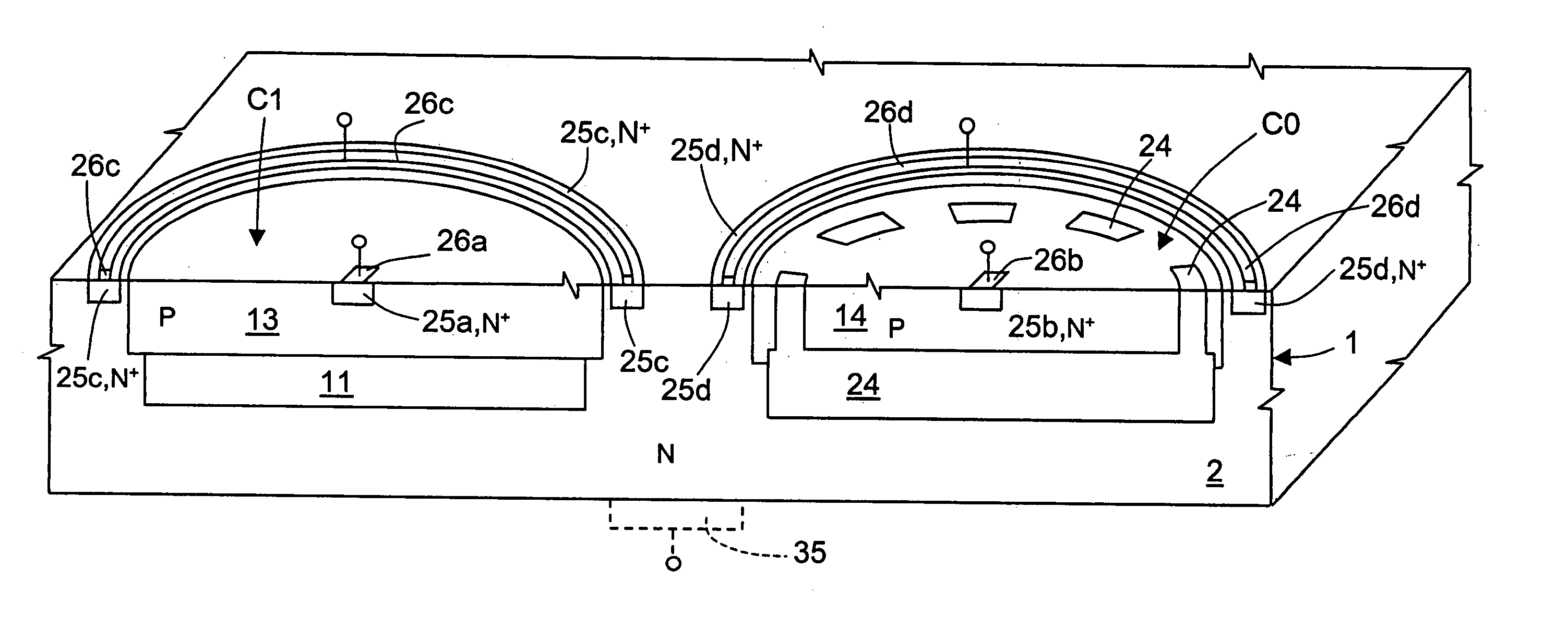
[0029] Hereinafter, an embodiment of a process for manufacturing a semiconductor material sensor of capacitive type is described. The present process is based upon the process disclosed in U.S. application Ser. No. 10 / 327,702 for manufacturing a SOI wafer, and, more precisely, refers to the second embodiment shown in FIGS. 11-14 of said document.

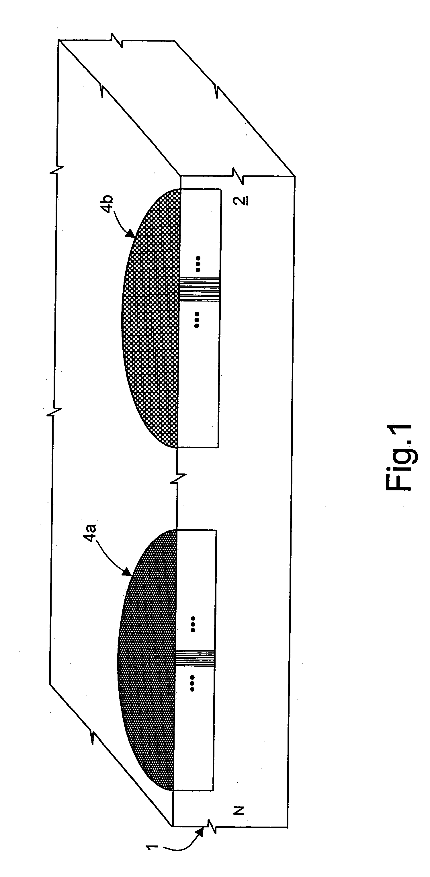
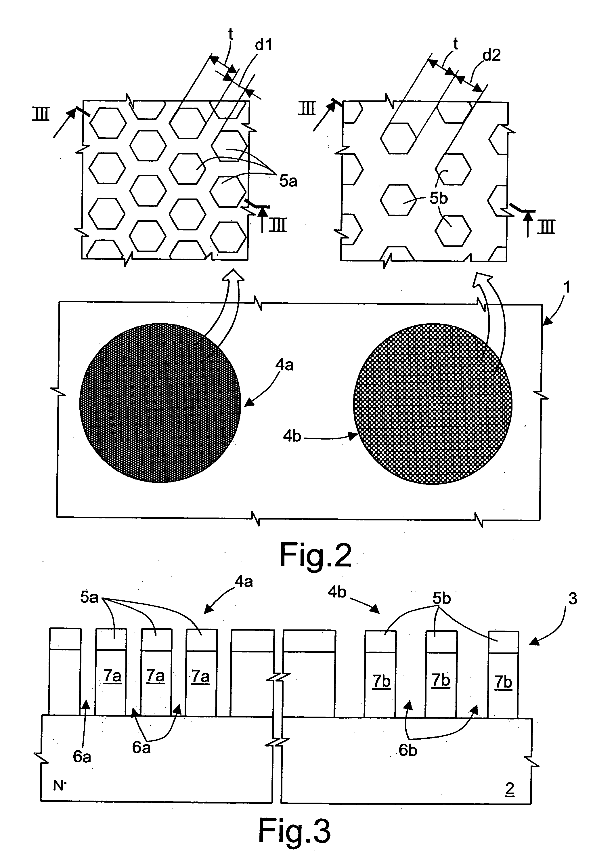
[0030]FIG. 1 shows a wafer 1 of semiconductor material, preferably monocrystalline silicon, comprising an N-type substrate 2, designed to form the bulk of the device. A resist mask 3 (visible in the enlarged detail of FIG. 3) is formed on the top surface of the substrate 2. The mask 3 has two circular areas, designated by 4a and 4b and hereinafter referred to as sensor area and reference area, respectively. In each of these areas, a honeycomb lattice is defined, the two lattices being of different sizes.

[0031] In particular, as appears in the enlarged detail of FIG. 2, the sensor area 4a has mask regions 5a with an hexagonal shape arranged...


PUM


Abstract

Method for manufacturing a semiconductor pressure sensor, wherein, in a silicon substrate, trenches are dug and delimit walls; a closing layer is epitaxially grown, that closes the trenches at the top and forms a suspended membrane; a heat treatment is performed so as to cause migration of the silicon of the walls and to form a closed cavity underneath the suspended membrane; and structures are formed for transducing the deflection of the suspended membrane into electrical signals.

Description

BACKGROUND OF THE INVENTION [0001] 1. Field of the Invention [0002] The subject of the present invention is a method for manufacturing a semiconductor pressure sensor. [0003] 2. Description of the Related Art [0004] As is known, a pressure sensor is a device that converts a variation in pressure into a variation of an electrical quantity (a resistance or a capacitance). In the case of a semiconductor sensor, the pressure variation is detected by a membrane of semiconductor material, which overlies a cavity and is able to undergo deflection under mechanical stress. [0005] Pressure sensors using semiconductor technology typically find their application in medicine, in household appliances, in consumer electronics (cell-phones, PDAs-Personal Digital Assistants-), and in the automotive field. In particular, in the latter sector, pressure sensors are used traditionally for detecting the pressure of the types of motor vehicles, and are used by the control unit for alarm signaling. Pressur...

Claims


Application Information

Patent Timeline
IPC IPC(8): G01L9/00H01L21/00
CPCG01L9/0073G01L9/0045
Inventor VILLA, FLAVIO FRANCESCOBARLOCCHI, GABRIELECORONA, PIETROVIGNA, BENEDETTOBALDO, LORENZO
Owner STMICROELECTRONICS SRL
Why Eureka
Try Eureka