Method for the formation of silicides

a technology of silicide and silicide, which is applied in the field of semiconductor device fabrication, can solve the problems of affecting the quality of these devices, short circuit between the gate and the source and/or drain active regions, and junction leakage, so as to reduce the resistance of the layer, the effect of limiting the channeling of ions

Inactive Publication Date: 2005-09-22
STMICROELECTRONICS SRL +1
View PDF12 Cites 3 Cited by
  • Summary
  • Abstract
  • Description
  • Claims
  • Application Information

AI Technical Summary

Benefits of technology

[0025] Metals that have the property of forming a silicide by thermal processing with silicon are, for example, Co, nickel (Ni), platinum (Pt) and titanium (Ti). Their corresponding silicides are CoSi2, PtSi, NiSi, and TiSi2 respectively. Such metals may be deposited, for example, by LPCVD (Low-Pressure Chemical Vapor Deposition) or by a sputtering process.
[0026] Advantageously, the implantation of step a) may take place through a dielectric layer, which makes it possible to limit the channeling of the ions into the silicon. This dielectric layer is removed during a removal step that comes between steps b) and c).
[0027] Moreover, the heat treatment of step b) has the function of repairing the defects generated in the structure owing to the ion implantation.
[0028] Step b) may be carried out by an annealing operation in order to activate dopant species pre-implanted in the silicon (especially in the source and drain regions of the MOS transistors of the wafer). Such an annealing step is conventional in the fabrication of an MOS transistor. In addition, since steps c) to e) also form part of the conventional siliciding process, implementation of the invention may therefore require only one additional step compared with the fabrication of an MOS transistor according to the prior art, namely the implantation step a).
[0029] In practice, with implantation of GE+ ions, it has been found that there is a reduction by a factor of 100 in junction leakage in an MOS transistor, compared with the implementation of a process according to the prior art.
[0030] By correctly choosing the implanted Ge+ ion dose, it is possible furthermore to reduce the layer resistances by 30%.

Problems solved by technology

MOS transistors are important components of semiconductor devices, and the electrical performance of the gate of the MOS transistors directly affects the quality of these devices.
However, such an Ar ion bombardment induces junction leakage.
In addition, it results in re-sputtering of silicon on the sidewalls of the spacers, which may result in a short circuit between the gate and the source and / or drain active regions (a phenomenon called “bridging”).
Finally, it also leads to degradation of the silicide spikes.
Furthermore, because of their spiking, the thickness of the silicide layers formed using the known techniques of the prior art is poorly controlled, essentially because it results from the conditions under which the actual siliciding step is carried out (temperature and duration of a siliciding heat treatment).

Method used


Image

  • Method for the formation of silicides
  • Method for the formation of silicides
  • Method for the formation of silicides

Examples


Embodiment Construction

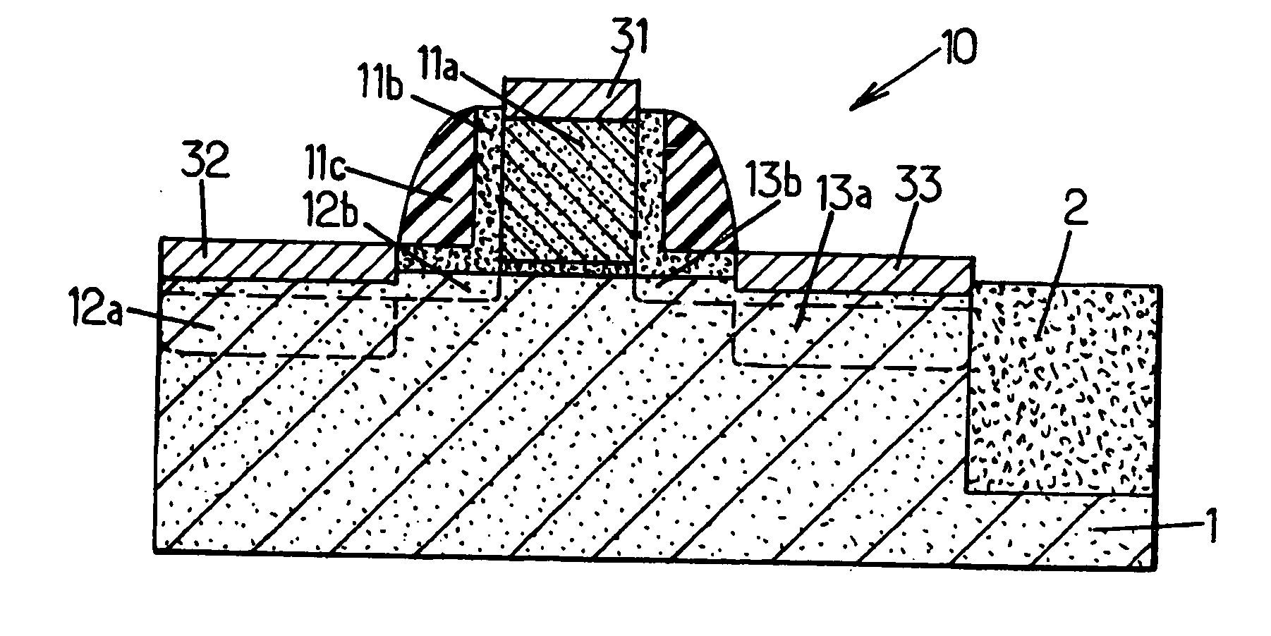
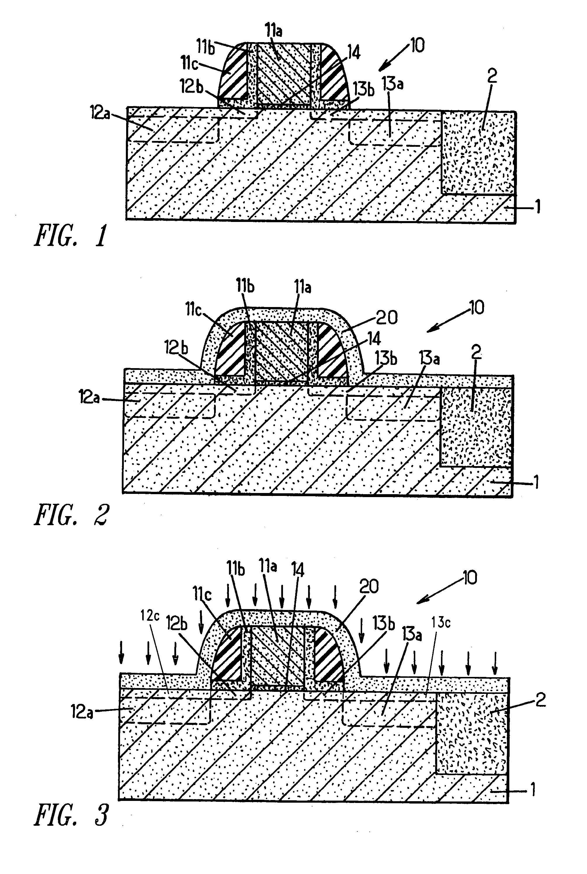
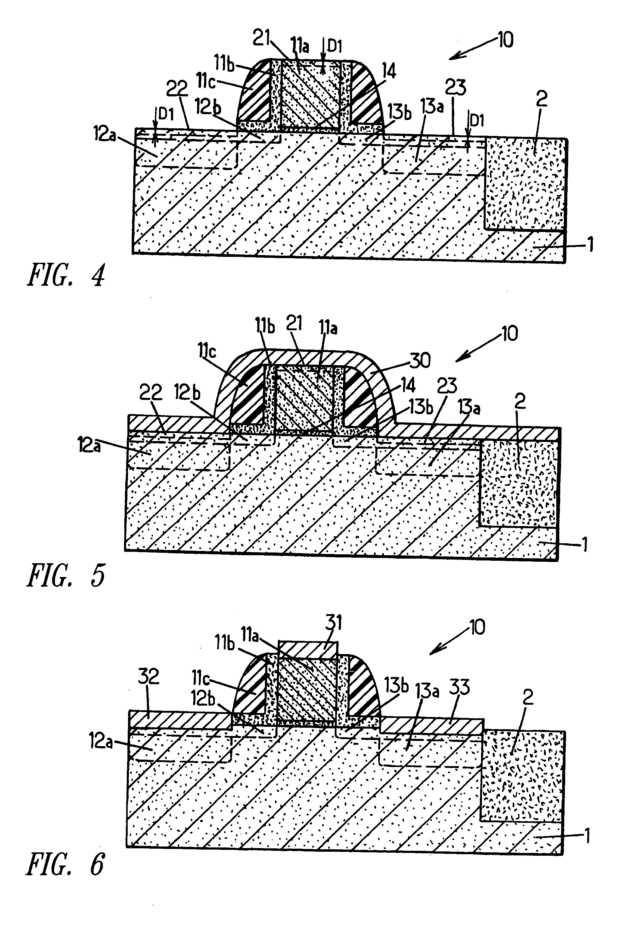
[0033] In the drawings, identical elements bear the same references. Each figure shows a sectional view of a transistor 10, which is an MOS transistor produced on the surface of a semiconductor wafer, forming a silicon substrate 1.

[0034] The diagram in FIG. 1 shows the transistor 10 before the start of the siliciding process according to the invention.

[0035] The gate of the transistor 10 comprises a polycrystalline silicon (polysilicon) layer 11 a or an amorphous silicon layer used as main conducting layer. The layer 11 a is attached to the surface of the substrate 1, from which it is isolated by a thin gate oxide layer 14, for example made of silicon dioxide (SiO2). The main conducting layer 11a and the layer of insulation 14 are surrounded by a nitride layer 11b lying perpendicular to the surface of the substrate 1. The layer 11b also includes a part lying parallel to the surface of the substrate 1, extending away from the layers 11a and 14. The nitride may be silicon nitride (S...


PUM

PropertyMeasurementUnit
thicknessaaaaaaaaaa
dielectricaaaaaaaaaa
electrical performanceaaaaaaaaaa

Abstract

A process for forming a silicide on top of at least one silicon portion on the surface of a semiconductor wafer, comprising the following steps: a) implanting, at a defined depth in the silicon portion, through a dielectric layer, of ions that have the property of limiting the silicidation of metals; b) performing heat treatment; c) depositing a metal layer, the metal being capable of forming a silicide by thermal reaction with the silicon; d) performing rapid thermal processing suitable for siliciding the metal deposited at step c); and e) removing the metal that has not reacted to the thermal processing of step d). Advantageously, the thickness of the silicide layer created at step d) is controlled by a suitable choice of the depth of the implantation carried out in step a).

Description

BACKGROUND OF THE INVENTION [0001] 1. Field of the Invention [0002] The present invention relates to the fabrication of semiconductor devices and more particularly to the formation of suicides by thermal reaction with silicon. [0003] The invention is especially applicable in the fabrication of MOS (Metal Oxide Semiconductor) transistors in all technologies using silicides, in particular in 0.18-μm, 0.12-μm, 90-nm, or 65-nm technologies. [0004] 2. Description of the Related Art [0005] MOS transistors are important components of semiconductor devices, and the electrical performance of the gate of the MOS transistors directly affects the quality of these devices. The gate of an MOS transistor typically comprises a polycrystalline silicon (polysilicon) layer or an amorphous silicon layer used as main conducting layer, and sometimes a silicide layer, for example a cobalt silicide (CoSi2) layer, stacked on the main conducting layer. Likewise the source and drain active regions of the MOS ...

Claims


Application Information

Patent Timeline
Patent Type & Authority Applications(United States)
IPC IPC(8): H01L21/265H01L21/28H01L21/285H01L21/336
CPCH01L21/26506H01L29/665H01L21/28518H01L21/28061
Inventor WACQUANT, FRANCOISREGNIER, CHRISTOPHEFROMENT, BENOITLENOBLE, DAMIENEL FARHANE, REBHA
Owner STMICROELECTRONICS SRL
Why Eureka
Try Eureka