Photo-detecting device

a technology of photodetecting and image sensor, which is applied in the direction of radiation control devices, semiconductor devices, picture signal generators, etc., can solve the problems of low efficiency of use of available light, reducing the color reproducibility of images, and light not being passed by the color filter, etc., to achieve higher quality imaging, reduce weight, and improve image quality

Active Publication Date: 2005-09-29
PANASONIC CORP
View PDF2 Cites 21 Cited by
  • Summary
  • Abstract
  • Description
  • Claims
  • Application Information

AI Technical Summary

Benefits of technology

[0008] In recent years, it has been required to provide a solid-state image sensor with higher performance, higher quality imaging, more reduction in weight, and the like.
[0009] However, the conventional solid-state image sensor selects red, green, blue light from light incident on each photo-detecting device using the color filter, so that light not being passed by the color filter is absorbed in the filter and wasted. This results in a problem that the conventional solid-state image sensor has low efficiency of use for available light in the photo-detecting device and eventually reduces color reproducibility of images, so that the conventional solid-state image sensor fails to meet the requirement of higher quality imaging.
[0010] In order to address the above problem, U.S. Pat. No. 5,965,875 discloses a photo-detecting device that enables to perform color separation of the incident light into the RGB primary colors without using the color filter. The disclosed photo-detecting device is formed by stacking a plurality of pn-junctions in silicon substrates which absorb red, green, and blue light separately, and performs color separation using the pn-junctions. Accordingly, efficiency of use for available light in the disclosed photo-detecting device is increased more than that in the photo-detecting device using the color filter. However, the disclosed photo-detecting device has a drawback that the light in one pn-junction is leaked into another pn-junction. As a result, color separation efficiency of the incident light in the disclosed photo-detecting device is decreased more than that in the photo-detecting device using the color filter. For example, blue light, which has not been converted into electric charges in a pn-junction of the top layer where blue light is converted, is leaked into a lower pn-junction where green light is converted.

Problems solved by technology

However, the conventional solid-state image sensor selects red, green, blue light from light incident on each photo-detecting device using the color filter, so that light not being passed by the color filter is absorbed in the filter and wasted.
This results in a problem that the conventional solid-state image sensor has low efficiency of use for available light in the photo-detecting device and eventually reduces color reproducibility of images, so that the conventional solid-state image sensor fails to meet the requirement of higher quality imaging.
However, the disclosed photo-detecting device has a drawback that the light in one pn-junction is leaked into another pn-junction.

Method used


Image

  • Photo-detecting device
  • Photo-detecting device
  • Photo-detecting device

Examples


Embodiment Construction

[0043] The following describes a MOS solid-state image sensor according to an embodiment of the present invention with reference to the drawings.

[0044]FIG. 3 is a cross-sectional view showing structures of a photo-detecting device in the MOS solid-state image sensor structures and its periphery, according to the present embodiment.

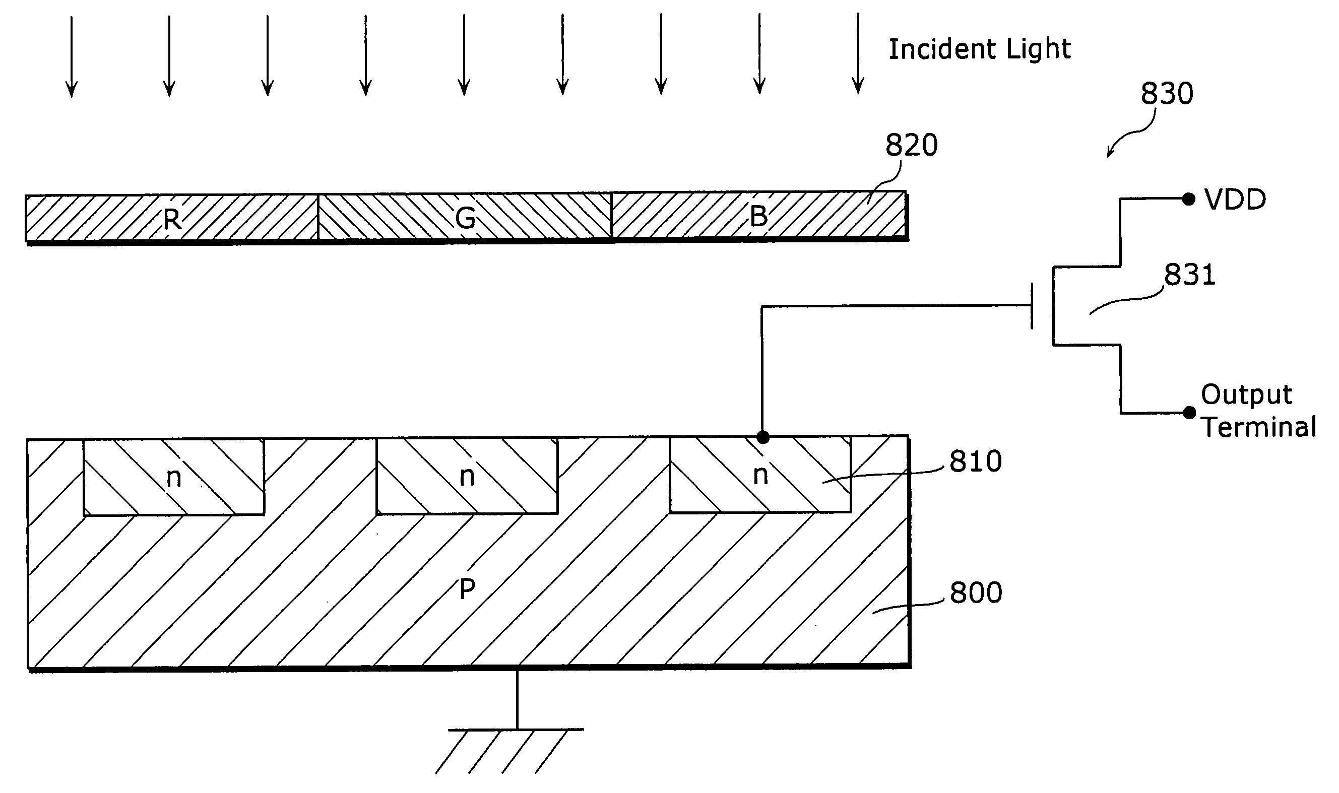
[0045] Referring now to FIG. 3, the solid-state image sensor according to the present embodiment is comprised of: a photo-detecting device 100; and output amplifiers 110 that have each MOS transistors, that are connected with the photo-detecting device 100, and that convert signal charges into voltage, and amplify and output the voltage.

[0046] The photo-detecting device 100 that includes bonding silicon-on-insulator (SOI) substrates is formed by sequentially stacking: a first silicon substrate 120; a first SOI substrate 130 in which a second silicon substrate 132 is formed on a first SOI insulation layer 131; and a second SOI substrate 140 in which a th...


PUM


Abstract

A photo-detecting device that enables a solid-state image sensor to meet the requirement of higher quality imaging including: a first silicon substrate 120 having p- and n-type regions; a first SOI substrate 130 in which a second silicon substrate 132 having p- and n-type regions is formed on a first SOI insulation layer 131; and a second SOI substrate 140 in which a third silicon substrate 142 having p- and n-type regions is formed on a second SOI insulation layer 141. Each pn-junction of the first silicon substrate 120, the second silicon substrate 132, and the third silicon substrate 142 forms a photodiode for converting incident light into electric charges. The depth of each pn-junction, which is measured from the surface of the second SOI substrate 140 irradiated with the light, is determined according to absorption length of light to be converted into electric charges.

Description

BACKGROUND OF THE INVENTION [0001] (1) Field of the Invention [0002] The present invention relates to a photo-detecting device, and more particularly to a photo-detecting device in a solid-state image sensor. [0003] (2) Description of the Related Art [0004] Charge-coupled device (CCD) or metal-oxide-semiconductor (MOS) solid-state image sensors are mounted on digital still cameras, camcorders, and the like. Such solid-state image sensors convert light incident on photo-detecting devices into electric charges. In the CCD solid-state image sensor, the generated signal charges are accumulated in potential wells, and then transferred. In the MOS solid-state image sensor, on the other hand, the generated signal charges are read out as voltage directly from the photo-detecting devices using MOS transistors. Imaging areas in those solid-state image sensors, in which the photo-detecting devices are two-dimensionally arranged, have red-green-blue (RGB) primary color filters with the Bayer or...

Claims


Application Information

Patent Timeline
Patent Type & Authority Applications(United States)
IPC IPC(8): H01L31/0352H01L27/146H01L31/0392H01L31/10H01L31/101H04N9/07
CPCH01L27/14609H01L31/035236H01L27/14687H01L27/14647
Inventor TAMAI, SEIICHIRO
Owner PANASONIC CORP
Why Eureka
Try Eureka