

Plasma display panel having electromagnetic wave shielding layer
a technology of electromagnetic wave shielding layer and display panel, which is applied in the direction of electrodes, identification means, instruments, etc., can solve the problems of inability to achieve efficient heat dissipation by air convection in space, difficulty in constructing air pathway large enough to circulate air, and increase manufacturing costs. , to achieve the effect of reducing manufacturing costs, improving heat radiation efficiency, and reducing manufacturing tim
- Summary
- Abstract
- Description
- Claims
- Application Information
AI Technical Summary
Benefits of technology
Problems solved by technology
Method used
Image

Examples
first embodiment
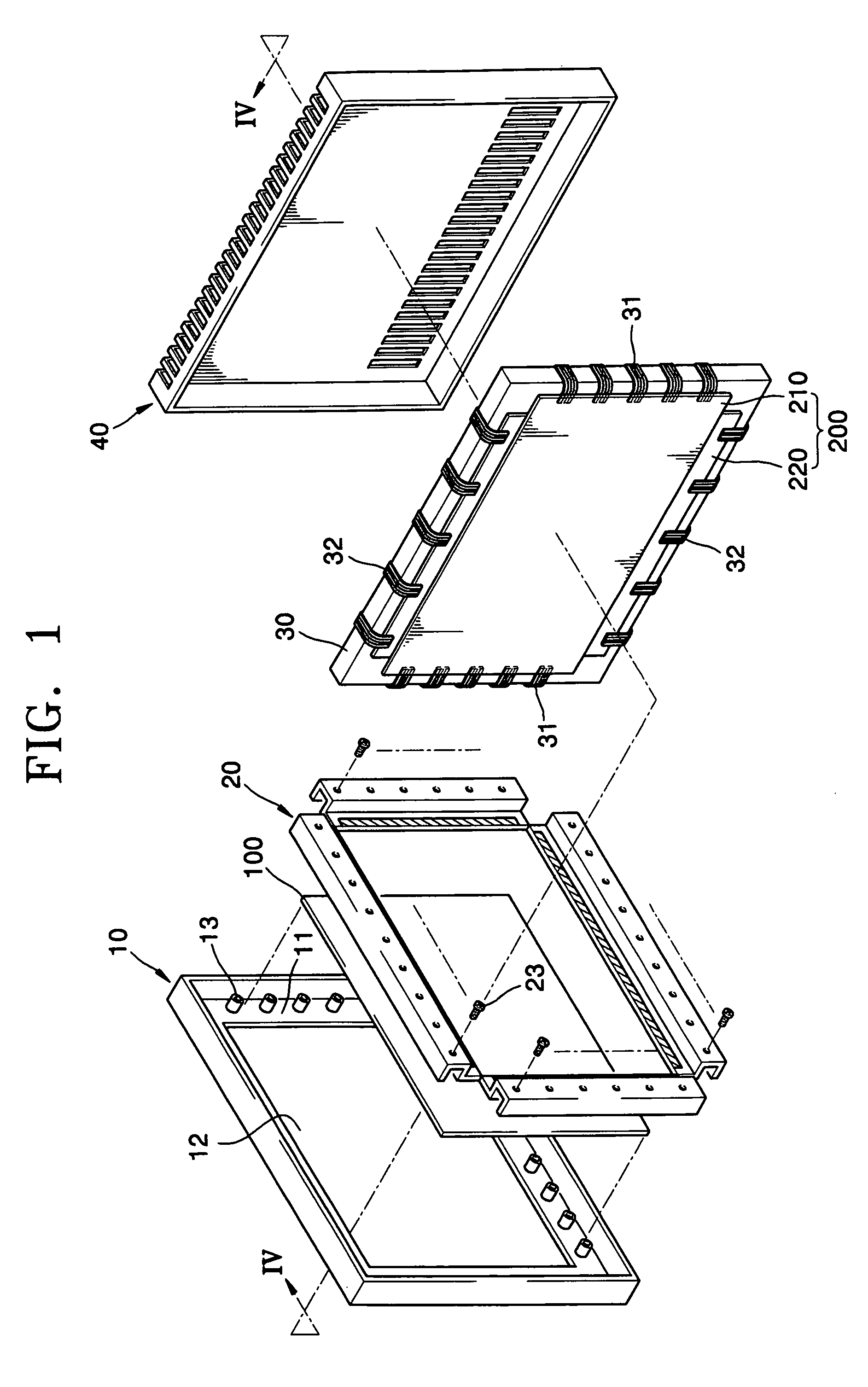
[0049]FIG. 5 is an exploded perspective view of a plasma display device having a PDP according to the present invention, and FIG. 6 is a cross-sectional view taken along line VI-VI of FIG. 5.
[0050] Referring to FIG. 5, a PDP 300 comprises a front case 10 that includes a perimeter unit 11 defining a window 12, a plasma display panel (PDP) 300 which includes a front panel 310 and a rear panel 220 and which is disposed on a rear of the front case 10, a chassis 30 that supports the PDP 300, connecting cables 31 and 32 which connect a circuit unit (not shown) that drives the PDP 300 and is disposed on a rear of the chassis 30 and the PDP 300, and a rear case 40 coupled to the front case 10 and disposed on a rear of the chassis 30. As depicted in FIG. 6, a thermal conductive sheet 230 is interposed between the PDP 300 and the chassis 30.
[0051] It can be seen, by comparing FIG. 1 and FIG. 5, that the plasma display device having the PDP 300 according to a first embodiment does not include...
second embodiment
[0103] As depicted in FIGS. 15 and 16, a PDP 400 according to the present invention includes a front panel 410 and a rear panel 420.
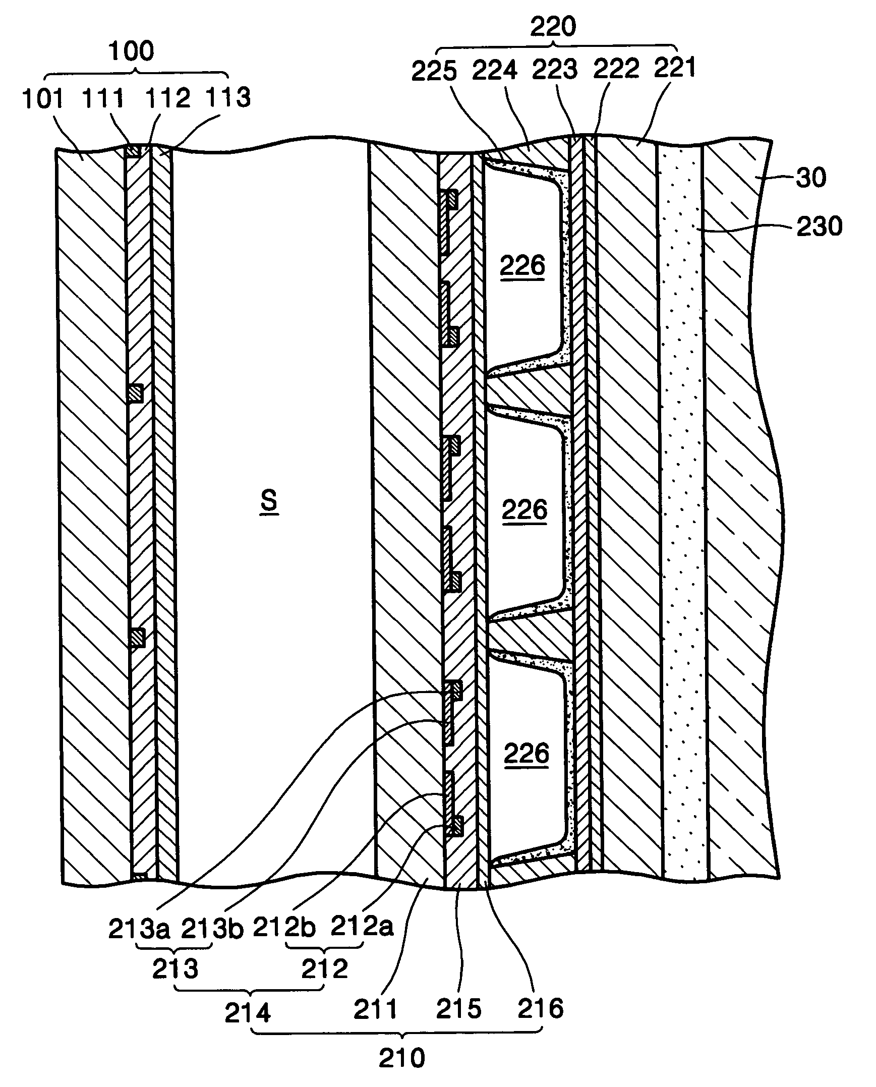
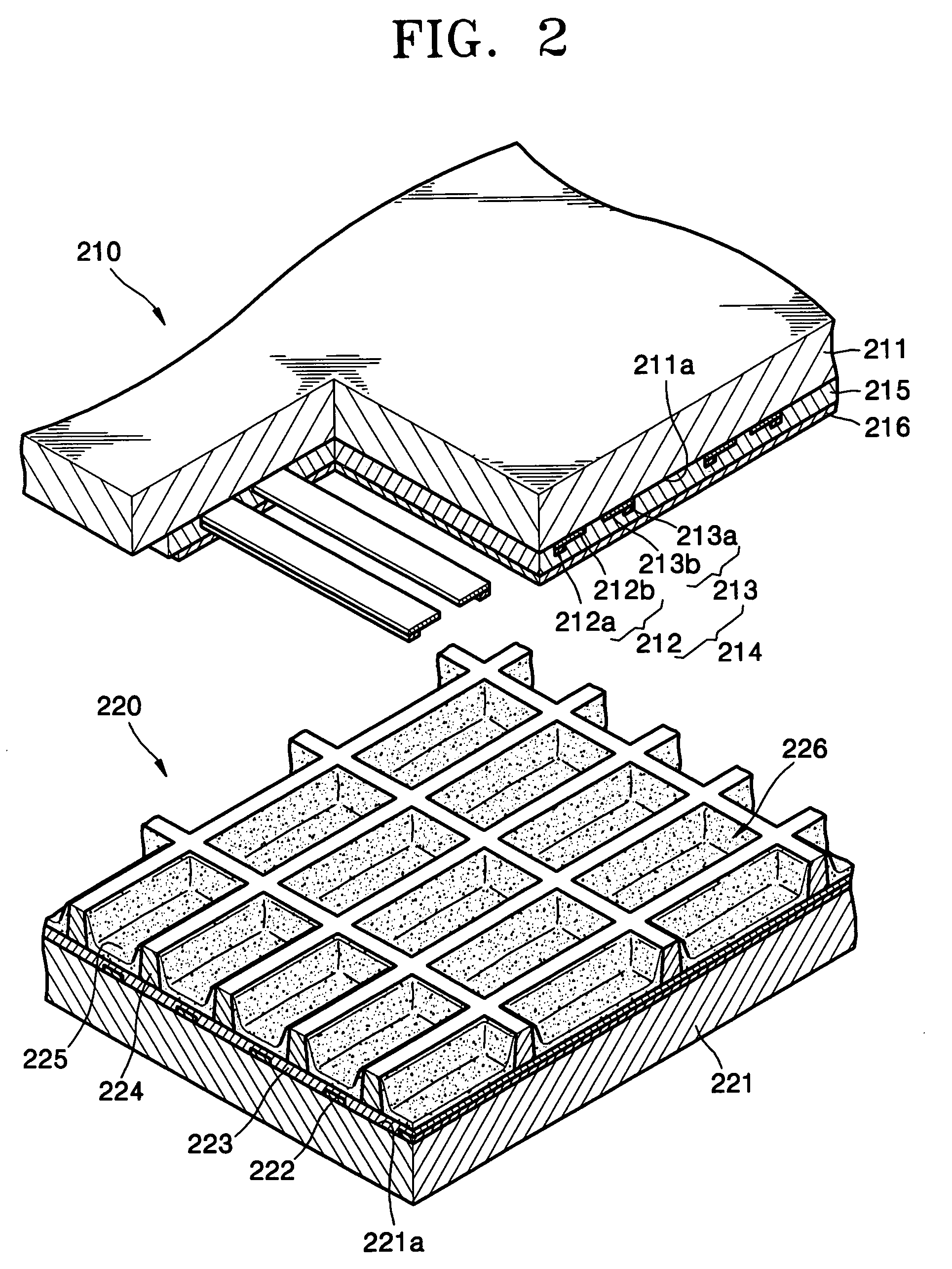
[0104] The front panel 410 comprises a front substrate 411, front barrier ribs 415 defining the discharge cells 426 and formed of a dielectric disposed on a rear surface 411b of the front substrate411, a plurality of front discharge electrodes 413 and rear discharge electrodes 412 embedded in the front barrier ribs 415 so as to surround the discharge cells 426, and an electromagnetic wave shielding layer 401 fixed on the front substrate 411. When necessary, the PDP 400 can further include a protection layer 416 that covers the front barrier ribs 415, a planarizing layer 402 the covers the electromagnetic wave shielding layer 401, and a near infrared ray shielding layer 403 formed on the planarizing layer 402. A discharge gas is filled in the discharge cells 426.
[0105] The rear panel 420 comprises a rear substrate 421 disposed parallel to the front subs...
PUM
 Abstract
Description
Claims
Application Information