Fabrication of nonpolar indium gallium nitride thin films, heterostructures and devices by metalorganic chemical vapor deposition

a technology of indium gallium nitride and thin film, which is applied in the direction of semiconductor devices, basic electric elements, electrical apparatus, etc., can solve the problems electronic devices, reducing the efficiency of carrier recombination, and qcse. undesirable, the effect of reducing the efficiency of iii-nitride based optoelectroni

Active Publication Date: 2005-09-29
JAPAN SCI & TECH CORP
View PDF29 Cites 382 Cited by
  • Summary
  • Abstract
  • Description
  • Claims
  • Application Information

AI Technical Summary

Problems solved by technology

However, conventional c-plane quantum well structures in III-nitride based optoelectronic and electronic devices suffer from the undesirable quantum-confined Stark effect (QCSE), due to the existence of strong piezoelectric and spontaneous polarizations.
The strong built-in electric fields along the c-direction cause spatial separation of electron and holes that in turn give rise to restricted carrier recombination efficiency, reduced oscillator strength, and red-shifted emission.
Unfortunately, nonpolar InGaN growth has proven challenging.
Sun, et al's, paper [Ref. 1] focused primarily on structural and photoluminescence characteristics of their material, and does not suggest that their InGaN film quality is sufficient to fabricate working devices.
However, the limited data given in the paper suggested their nonpolar InGaN material quality was extremely poor.
Indeed, their device displayed large shifts in emission intensity with varying injection current, poor diode current-voltage characteristics, and extreme detrimental heating effects that necessitated pulsing the current injection in order to test the device.
These poor characteristics most likely can be explained by deficient material quality.
First, the large lattice mismatches between InGaN and available substrates severely complicate InGaN heteroepitaxy.
Unfortunately, nonpolar nitrides are typically grown above 900° C. and more often above 1050° C., temperatures at which In readily desorbs from the surface.

Method used


Image

  • Fabrication of nonpolar indium gallium nitride thin films, heterostructures and devices by metalorganic chemical vapor deposition
  • Fabrication of nonpolar indium gallium nitride thin films, heterostructures and devices by metalorganic chemical vapor deposition
  • Fabrication of nonpolar indium gallium nitride thin films, heterostructures and devices by metalorganic chemical vapor deposition

Examples


Embodiment Construction

[0033] In the following description of the preferred embodiment, reference is made to the accompanying drawings which form a part hereof, and in which is shown by way of illustration a specific embodiment in which the invention may be practiced. It is to be understood that other embodiments may be utilized and structural changes may be made without departing from the scope of the present invention.

[0034] Overview

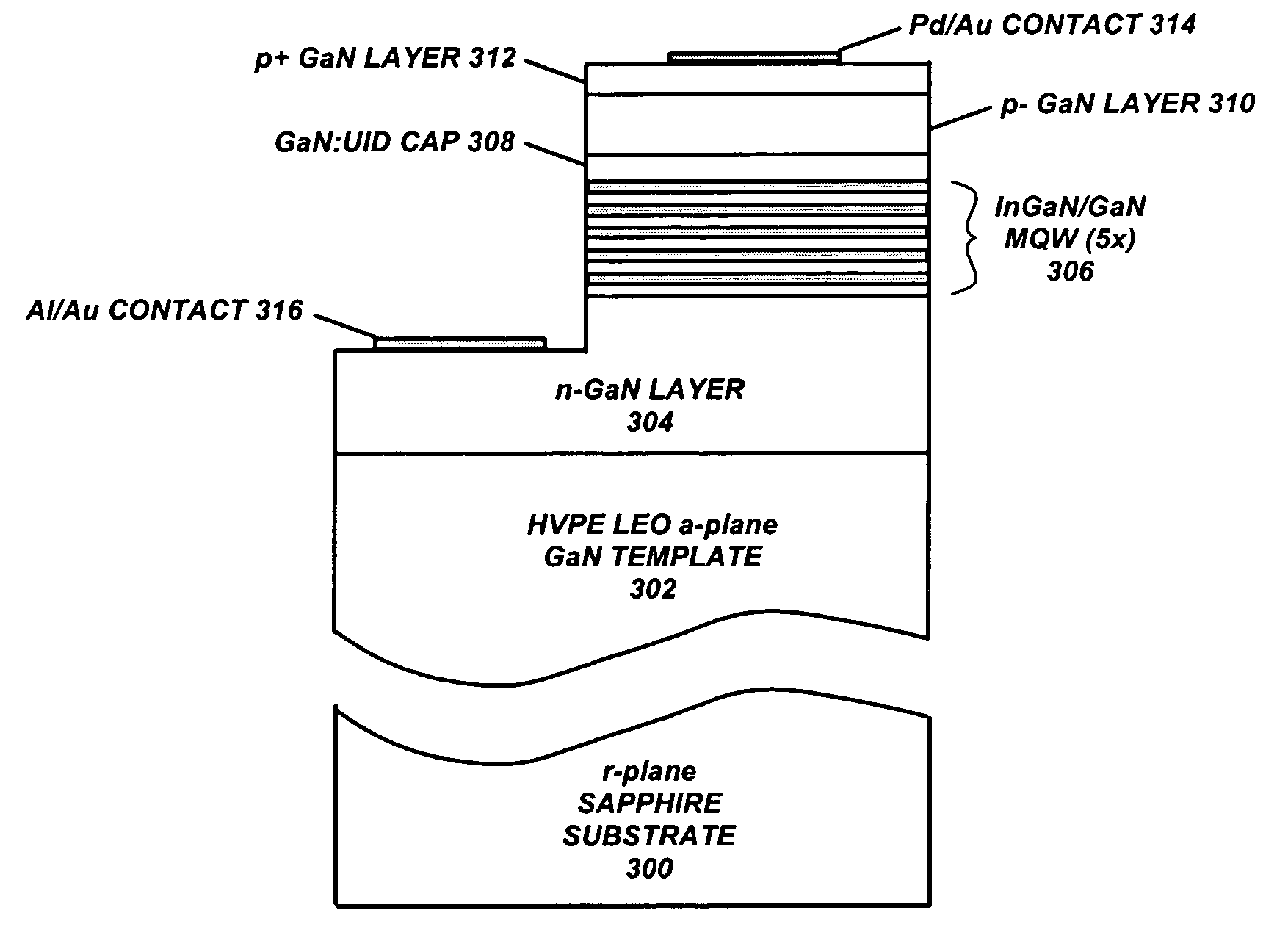
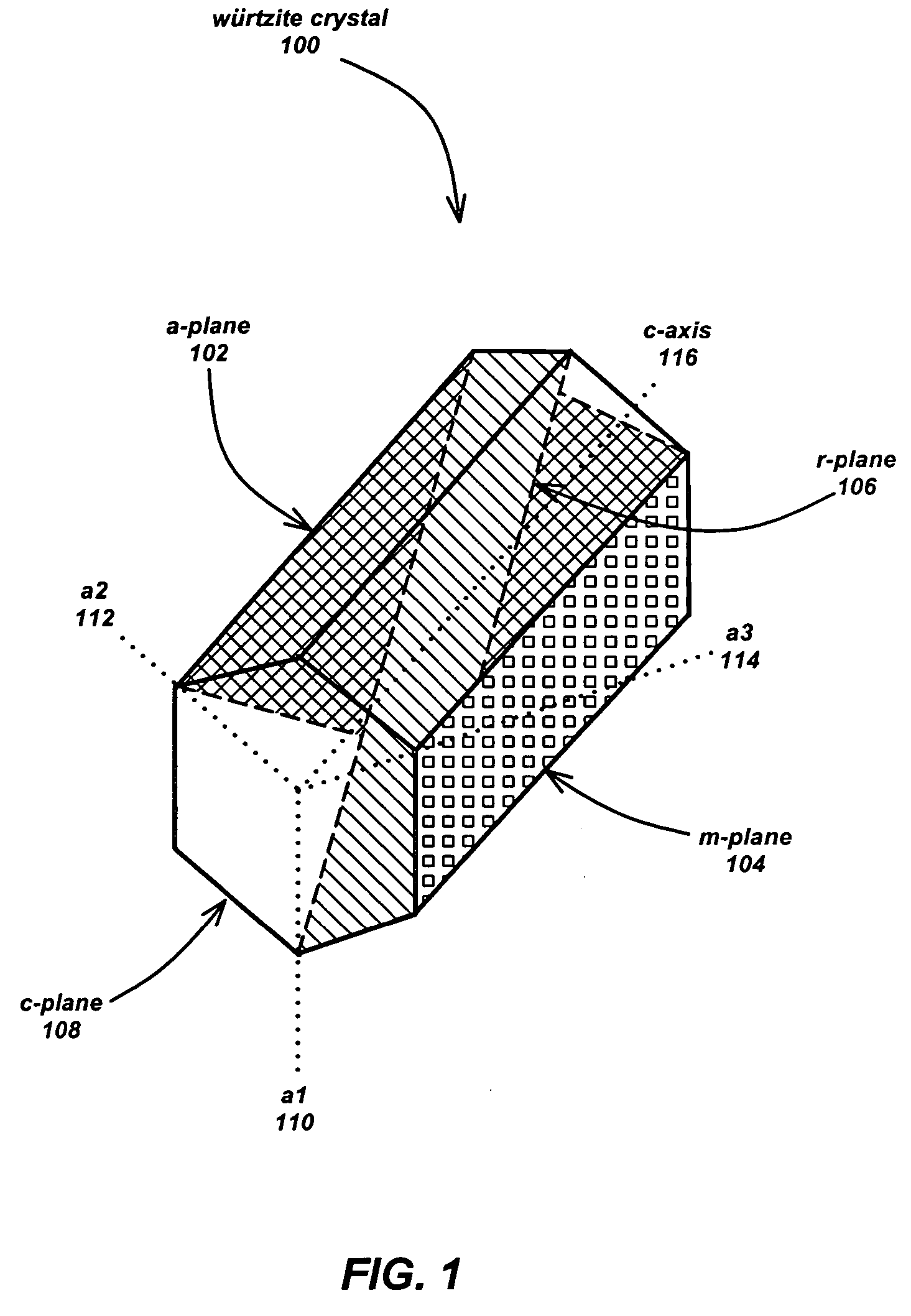
[0035] Growth of nonpolar nitride semiconductors offers a means of eliminating polarization effects in würtzite-structure III:nitride devices. Current (Ga,Al,In,B)N devices are grown in the polar [0001] c-direction, which results in charge separation across heterostructures. The resulting polarization fields are detrimental to the performance of current state of the art devices, particularly for optoelectronic devices. Growth of such devices along a nonpolar direction could significantly improve device performance.

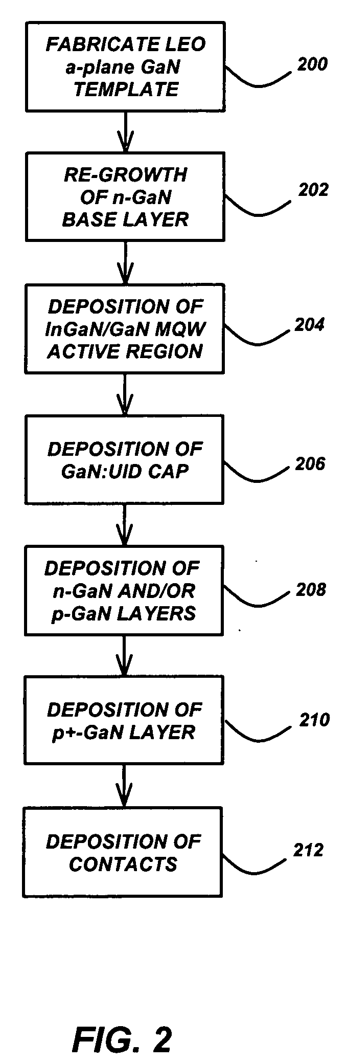
[0036] Until now, no means existed for growing high-qualit...


PUM

PropertyMeasurementUnit
temperatureaaaaaaaaaa
temperaturesaaaaaaaaaa

Abstract

A method for the fabrication of nonpolar indium gallium nitride (InGaN) films as well as nonpolar InGaN-containing device structures using metalorganic chemical vapor deposition (MOVCD). The method is used to fabricate nonpolar InGaN / GaN violet and near-ultraviolet light emitting diodes and laser diodes.

Description

CROSS-REFERENCE TO RELATED APPLICATIONS [0001] This application claims the benefit under 35 U.S.C. § 19(e) of the following co-pending and commonly-assigned U.S. patent application: [0002] U.S. Provisional Patent Application Ser. No. 60 / 569,749, filed on May 10, 2004, by Arpan Chakraborty, Benjamin A. Haskell, Stacia Keller, James S. Speck, Steven P. DenBaars, Shuji Nakamura and Umesh K. Mishra, entitled “FABRICATION OF NONPOLAR InGaN THIN FILMS, HETEROSTRUCTURES AND DEVICES BY METALORGANIC CHEMICAL VAPOR DEPOSITION,” attorneys' docket no. 30794.117-US-P1; [0003] which application is incorporated by reference herein. [0004] This application is related to the following co-pending and commonly-assigned applications: [0005] International Patent Application No. PCT / US03 / 21918, filed Jul. 15, 2003, by Benjamin A. Haskell, Michael D. Craven, Paul T. Fini, Steven P. DenBaars, James S. Speck, and Shuji Nakamura, entitled “GROWTH OF REDUCED DISLOCATION DENSITY NON-POLAR GALLIUM NITRIDE BY HY...

Claims


Application Information

Patent Timeline
Patent Type & Authority Applications(United States)
IPC IPC(8): H01L21/20H01L21/205H01L29/15H01L31/0312H01L33/00
CPCH01L21/02378H01L21/02389H01L21/0242H01L21/02433H01L21/02458H01L21/02502Y10S438/938H01L21/02609H01L21/0262H01L21/02647H01L33/0075H01L33/18H01L21/0254
Inventor CHAKRABORTY, ARPANHASKELL, BENJAMIN A.KELLER, STACIASPECK, JAMESDENBAARS, STEVEN P.NAKAMURA, SHUJIMISHRA, UMESH KUMAR
Owner JAPAN SCI & TECH CORP
Why Eureka
Try Eureka