Crystallization apparatus, crystallization method, device, optical modulation element, and display apparatus
a crystallization method and crystallization method technology, applied in the field of crystallization apparatus, can solve problems such as uneven display, and achieve the effect of large particle size and sufficient crystal growth
- Summary
- Abstract
- Description
- Claims
- Application Information
AI Technical Summary
Benefits of technology
Problems solved by technology
Method used
Image

Examples
first embodiment
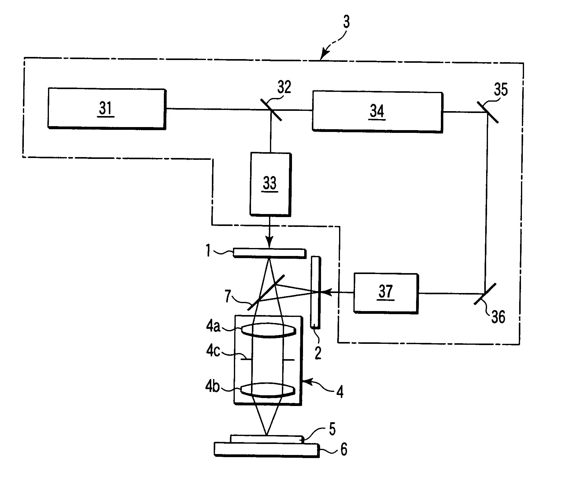
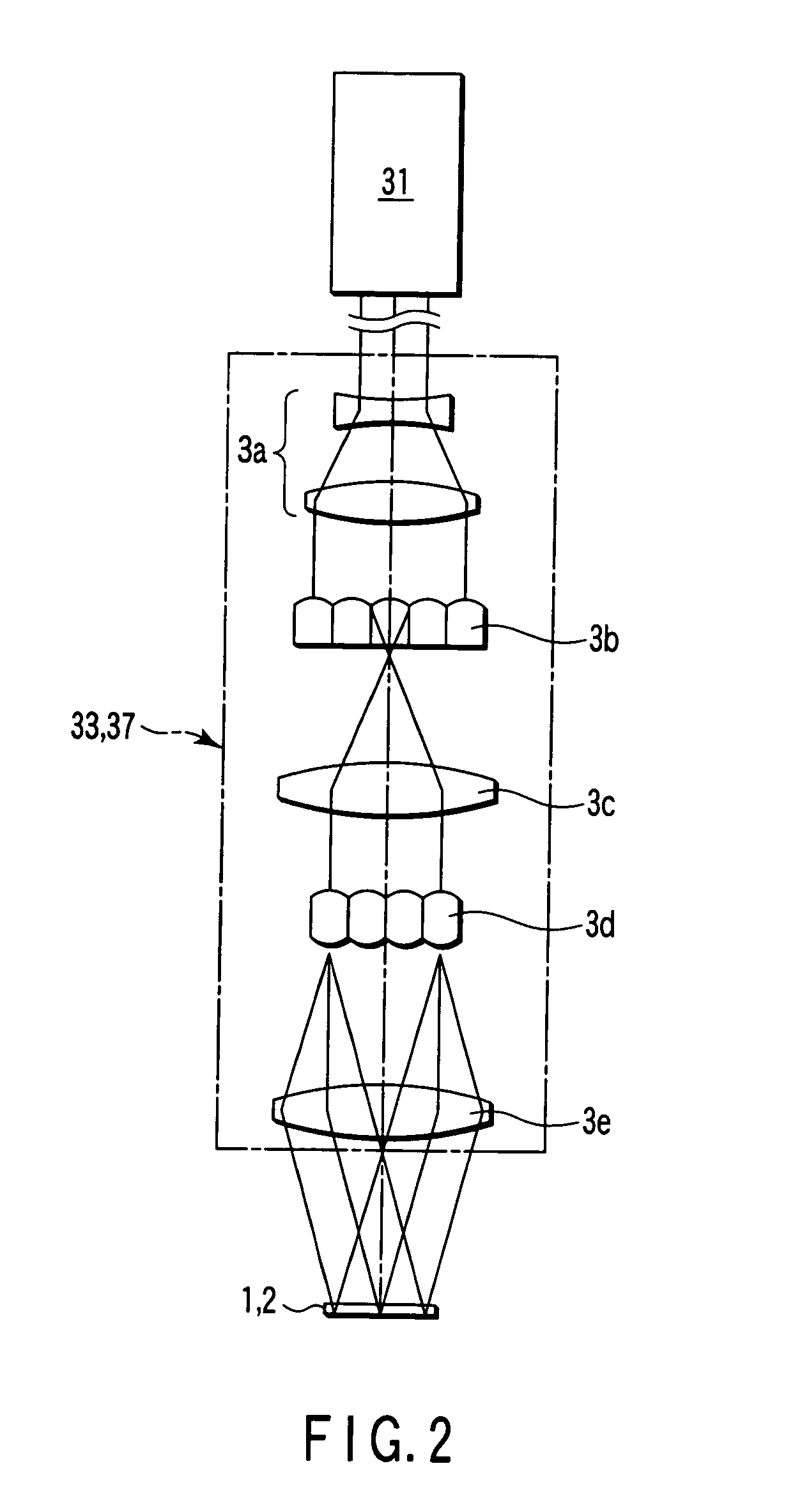
[0067]FIG. 1 is a view schematically showing a structure of a crystallization apparatus according to the present invention. FIG. 2 is a view schematically showing internal structures of a first illumination optical system and a second illumination optical system.
[0068] Referring to FIG. 1, the crystallization apparatus according to the first embodiment comprises a first optical modulation element 1 and a second optical modulation element 2 each of which modulates a phase of an incident light beam, an illumination system 3, an image formation optical system 4, and a substrate stage 6 on which a processed substrate 5 is mounted.
[0069] The detailed structures and effects of the first optical modulation element 1 and the second optical modulation element 2 will be described later. The illumination system 3 includes a KrF excimer laser light source 31 which supplies a pulse laser light having a wavelength of, e.g., 248 nm as a light source which outputs an energy light which melts a non...
third embodiment
[0084] Comparing the light intensity distributions shown in FIGS. 3B and 4B, it can be understood that a gradient of the light intensity distribution having the central peak share formed by using the second optical modulation element 2 is larger than a gradient of the chevron light intensity distribution in the V-shape formed by using the first optical modulation element 1. The light intensity distributions shown in these drawings are calculated on the assumption that a wavelength λ of a light is 248 nm, an image side numeral aperture NA of the image formation optical system 4 is 0.13, and a value σ (a coherence factor) of the image formation optical system 4 is 0.5. The calculation of a light intensity distribution presumes the same conditions.
[0085]FIGS. 5A and 5B are views schematically showing pulse light emission characteristics of the light source in the first embodiment, and a temporal relationship between the first pulse light which enters the first optical modulation eleme...
second embodiment
[0096] In the second embodiment, the first shaping optical system 41 which magnifies a diameter of the first laser light with a first magnifying power and the common illumination optical system 44 constitute a first illumination optical system which causes the first pulse light having a first angular distribution (an angular width) to enter the common optical modulation element 10. Further, the second shaping optical system 43 which magnifies a diameter of the second laser light with a second magnifying power smaller than the first magnifying power and the common illumination optical system 44 constitute a second illumination optical system which causes the second pulse light having a second angular distribution (an angular width) different from the first angular distribution to enter the common optical modulation element 10. As shown in FIG. 8A, the first shaping optical system 41 has a negative lens group 3f and a positive lens group 3g in the order from the light source. Likewise...
PUM
 Abstract
Description
Claims
Application Information
 - R&D
- Intellectual Property
- Life Sciences
- Materials
- Tech Scout
- Unparalleled Data Quality
- Higher Quality Content
- 60% Fewer Hallucinations
Browse by: Latest US Patents, China's latest patents, Technical Efficacy Thesaurus, Application Domain, Technology Topic, Popular Technical Reports.
© 2025 PatSnap. All rights reserved.Legal|Privacy policy|Modern Slavery Act Transparency Statement|Sitemap|About US| Contact US: help@patsnap.com