Semiconductor wafer and manufacturing method therefor

Inactive Publication Date: 2005-10-06
YAMAHA CORP
View PDF14 Cites 6 Cited by
  • Summary
  • Abstract
  • Description
  • Claims
  • Application Information

AI Technical Summary

Benefits of technology

[0031] It is an object of the invention to provide a semiconductor wafer and a manufacturing method therefor, which reduces nonuniformity of resist application in IC regions by reducing height differences between IC re

Problems solved by technology

This causes unwanted deviations of shapes and dimensions of thin-film elements.
In addition, there is a possibility that contaminating substances produced by thin-film elements may have adverse effects on the ‘exposed’ silicon-related portions of IC regions.
This causes problems in that wiring layers become very thin in proximity to edges of openings and are therefore easy to break compared with normal wiring layers formed in semiconductor devices.
However, it may be difficult to eliminate height differences betwee

Method used


Image

  • Semiconductor wafer and manufacturing method therefor
  • Semiconductor wafer and manufacturing method therefor
  • Semiconductor wafer and manufacturing method therefor

Examples


first embodiment

1. First Embodiment

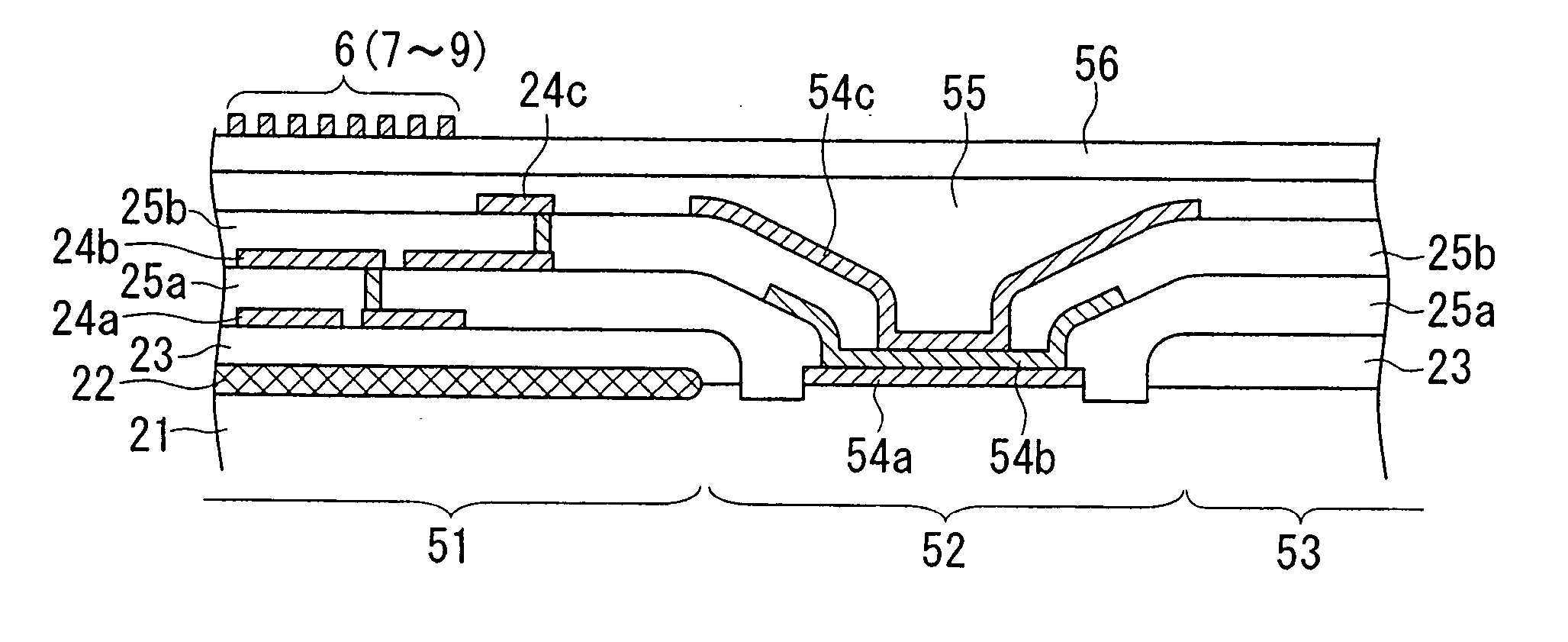
[0080]FIG. 1 is a cross-sectional view showing essential parts of a silicon wafer (or a semiconductor wafer) in which a plurality of semiconductor devices (i.e., semiconductor chips having magnetic sensors) are formed in accordance with a first embodiment of the invention, wherein parts identical to those shown in FIG. 7 are designated by the same reference numerals.

[0081] In FIG. 1, reference numeral 51 designates an IC that is formed in an IC region of the p-type silicon substrate 21; reference numeral 52 designates a seal ring that is formed in the periphery of the IC 51; and reference numeral 53 designates a scribing line (or a scribing region) that is formed outside of the seal ring 52 in the boundary between adjacent IC regions.

[0082] An insulating layer 23 composed of silicon dioxide (SiO2) is formed to cover the IC 51 and the scribing line 53 on the p-type silicon substrate 21; a wiring layer 24a having a prescribed wiring pattern composed of prescribed ...

second embodiment

2. Second Embodiment

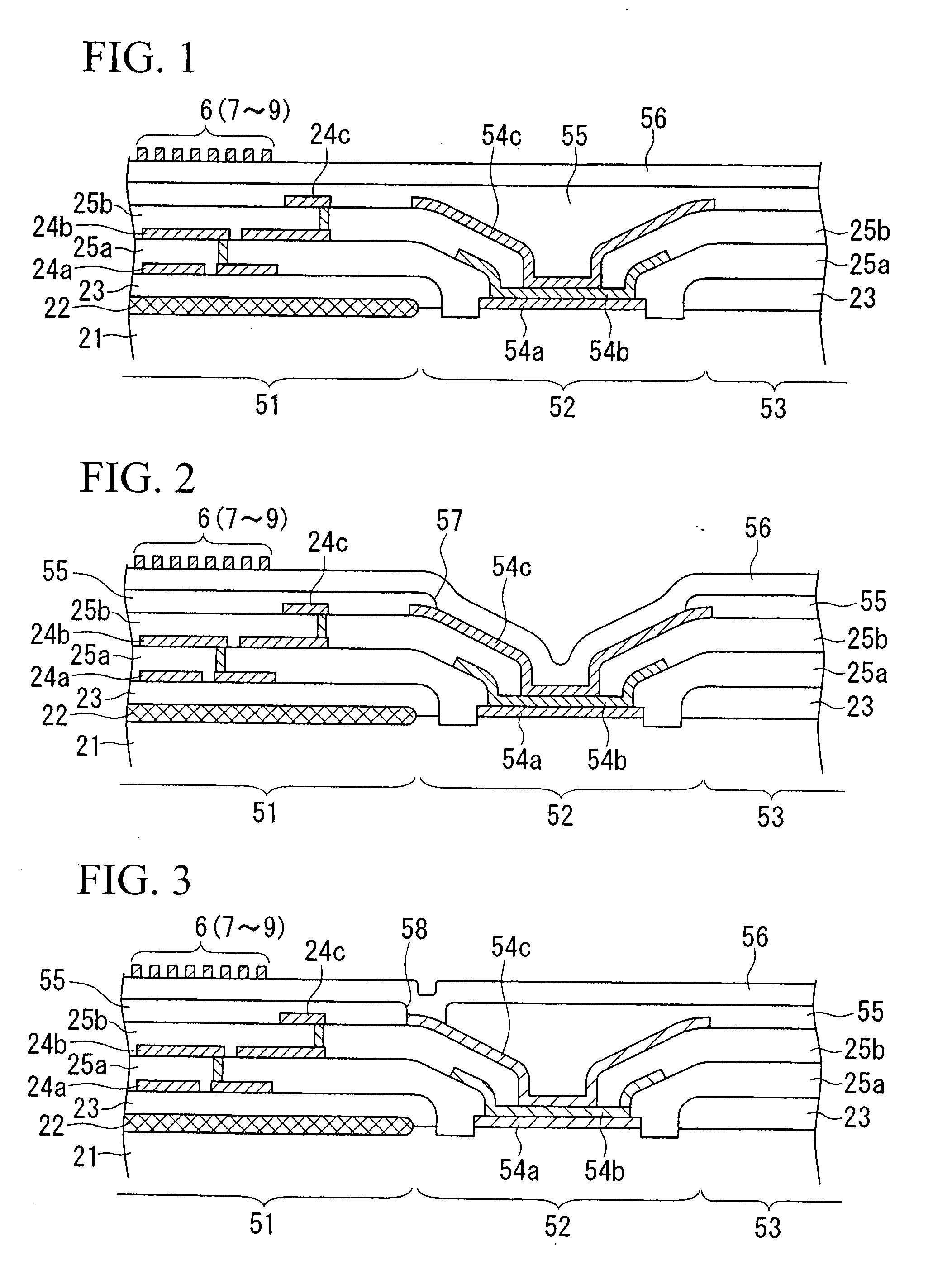
[0123]FIG. 10 is a cross-sectional view showing essential parts of a semiconductor device having thin-film elements in accordance with a second embodiment of the invention, wherein reference numeral 121 designates a p-type silicon substrate (or a semiconductor substrate); reference numerals 122 designate transistors formed on the silicon substrate; and reference numerals 123 designate field insulating films composed of silicon oxide, which are formed between the transistors 122. Herein, an IC region 124 includes the transistors 122, field insulating films 123, and peripheral circuits and other elements (not shown), which are formed on the silicon substrate 121.

[0124] The transistors 122 are each constituted by sources 131a and drains 131b, which are formed at upper ends of n+ embedded layers 130 formed on the silicon substrate 121, and gates 131d that are formed above the sources 131a and drains 131b via SiO2 films (or insulating films) 131c.

[0125] On the IC re...

third embodiment

3. Third Embodiment

[0154]FIG. 15 is a cross sectional view showing essential parts of a semiconductor device having thin films in accordance with a third embodiment of the invention, wherein parts identical to those shown in FIG. 10 are designated by the same reference numerals; hence, the detailed description thereof is omitted. Compared with the semiconductor device of the second embodiment shown in FIG. 10 in which the wiring layer 139 for establishing electric connection between the second wiring layer 135 and a thin-film element (not shown) is formed in the openings 136a to 138a, the semiconductor device of the third embodiment shown in FIG. 15 is characterized in that it includes a thin-film element section 160, in which the wiring layer 139 for establishing electric connection between the second wiring layer and a thin-film element (not shown) is formed in the openings 136a to 138a, and an external-terminal connection pad 170 in which an external-terminal electrode 180 is for...


PUM


Abstract

A plurality of IC regions are formed on a semiconductor wafer, which is cut into individual chips incorporating ICs, wherein wiring layers and insulating layers are sequentially formed on a silicon substrate. In order to reduce height differences between ICs and scribing lines, a planar insulating layer is formed to cover the overall surface with respect to ICs, seal rings, and scribing lines. In order to avoid occurrence of breaks and failures in ICs, openings are formed to partially etch insulating layers in a step-like manner so that walls thereof are each slanted by prescribed angles ranging from 20° to 80°. For example, a first opening is formed with respect to a thin-film element section, and a second opening is formed with respect to an external-terminal connection pad.

Description

CROSS-REFERENCE TO RELATED APPLICATIONS [0001] This application is a continuation-in-part of U.S. patent application Ser. No. 11 / 039,956, filed Jan. 24, 2005, the entirety of which is incorporated herein by reference.BACKGROUND OF THE INVENTION [0002] 1. Field of the Invention [0003] This invention relates to semiconductor wafers and to manufacturing methods therefor, in which integrated circuits are formed on semiconductor wafers, which are cut into individual chips along scribing lines. This invention also relates to semiconductor devices having thin-film elements, which are formed on semiconductor wafers, and to manufacturing methods therefor. [0004] This application claims priority on Japanese Patent Applications Nos. 2004-94621, 2004-94622 and 2005-75554, the contents of which are incorporated herein by reference. [0005] 2. Description of the Related Art [0006] Conventionally, semiconductor devices such as IC chips and LSI chips are manufactured using semiconductor wafers such ...

Claims


Application Information

Patent Timeline
IPC IPC(8): H01L21/00H01L21/4763H01L21/768H01L21/78H01L23/00H01L23/12H01L23/58H01L27/00H01L43/08H01L43/12
CPCH01L21/76801H01L21/76804H01L21/76819H01L21/7684H01L21/78H01L2924/0002H01L23/564H01L23/585H01L2924/00E02D29/02E02D2600/20E02D2600/40
Inventor NAITO, HIROSHI
Owner YAMAHA CORP
Why Eureka
Try Eureka