Silicon light waveguide with mos capacitors positioned on the waveguide

a technology of mos capacitors and light waveguides, which is applied in the direction of optical waveguide light guides, instruments, optics, etc., can solve the problem that the inventors have not previously used the plasma dispersion effect of mos capacitor structures for the mode control of optical waveguides

Inactive Publication Date: 2005-10-06
YISSUM RES DEV CO OF THE HEBREWUNIVERSITY OF JERUSALEM LTD
View PDF4 Cites 24 Cited by
  • Summary
  • Abstract
  • Description
  • Claims
  • Application Information

AI Technical Summary

Benefits of technology

[0010] The present invention is concerned with providing electro-optical devices based on the electrical field eff

Problems solved by technology

However, no previous work on the use of the plasma dispersion effect in MOS capacit

Method used


Image

  • Silicon light waveguide with mos capacitors positioned on the waveguide
  • Silicon light waveguide with mos capacitors positioned on the waveguide
  • Silicon light waveguide with mos capacitors positioned on the waveguide

Examples


Embodiment Construction

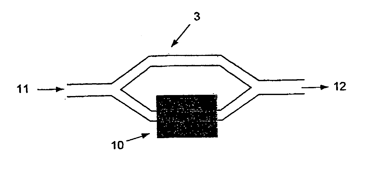
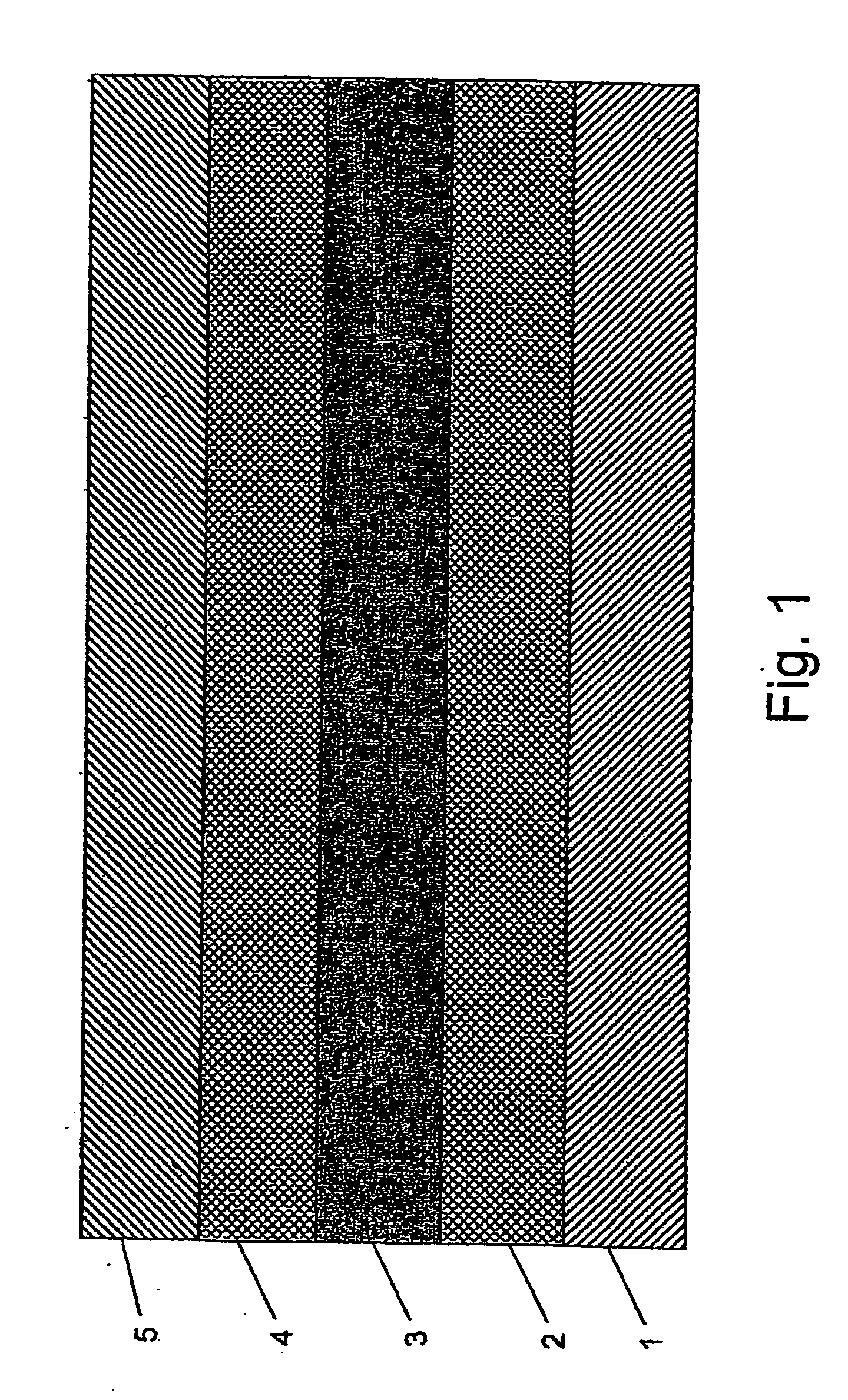
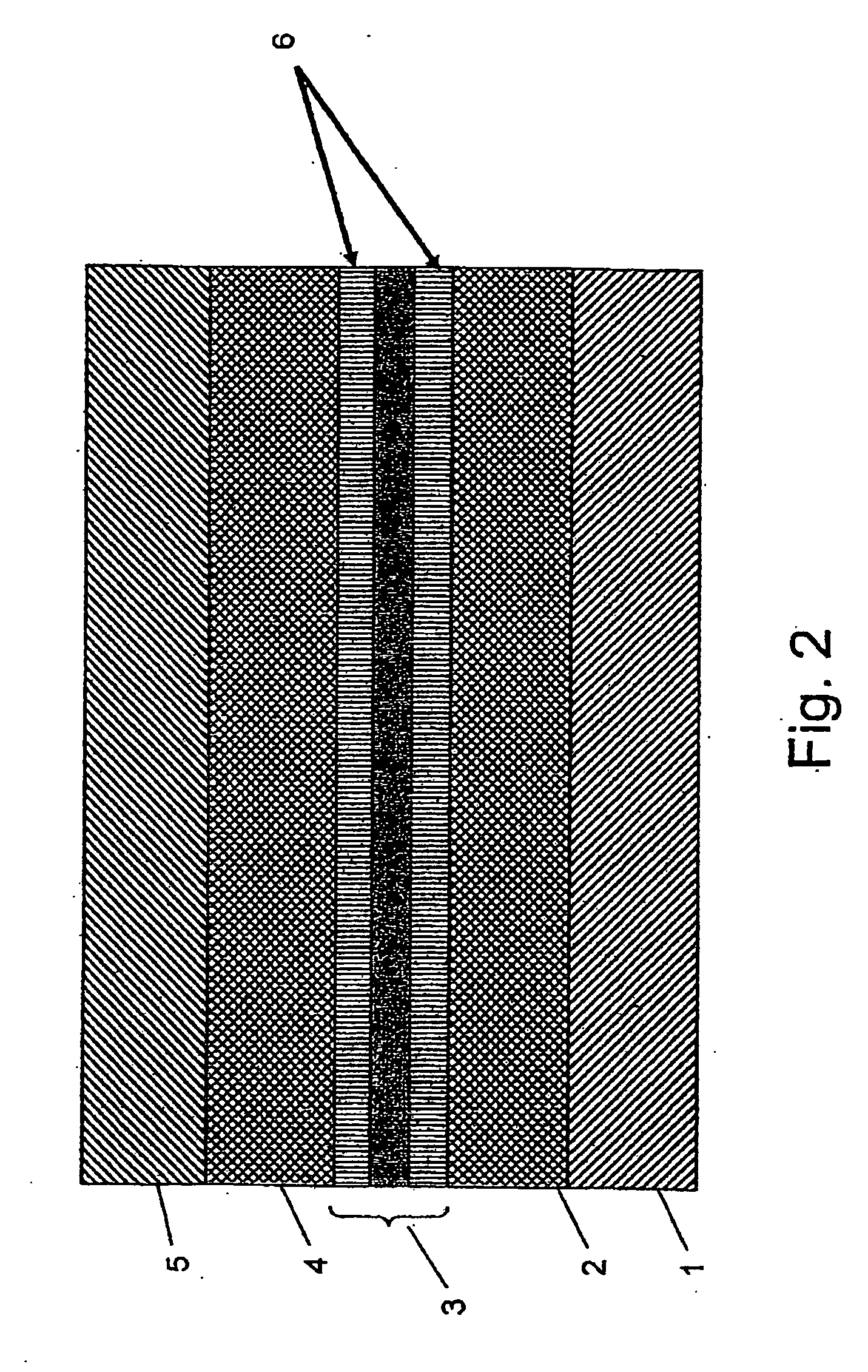
[0058]FIG. 1 is a schematic side view of the basic structure of the invention. A silicon waveguide 3 is created in the upper layer of a SOI (silicon on insulator) wafer. The lower two layers of the SOI wafer being the silicon substrate 1 and the silicon dioxide layer 2. Above the waveguide is a silicon dioxide upper cladding 4 and above the upper cladding a poly-silicon layer 5 is deposited and patterned to form a poly-silicon electrode. Skilled persons will recognize that any other type of conductive layer may be substituted for the poly-silicon layer.

[0059] This basic structure is farther processed in order to make electrical contacts to the substrate, the buried silicon wave-guide and the poly-silicon top layer, which may be covered with a protective layer (not shown in the figures) if desired. This protective layer may be of any suitable dielectric, including oxide.

[0060] On application of a potential difference to the silicon wave-guide, relative to the poly-silicon and / or th...


PUM


Abstract

The present invention provides a silicon wave-guide (3), with a silicon oxide cladding (2, 4) on a silicon substrate (1). At predetermined positions along the length of the wave-guide, are created metal oxide semiconductor (MOS) structures. A poly-silicon, or any other conductive layer (5), is deposited and patterned above the upper cladding (4) and electrical contacts are made to the substrate (1), the silicon wave-guide (3), and the poly-silicon layer (5). Upon the application of a potential difference between at least two of the layers from the group comprising the substrate (1), the silicon wave-guide (3), and the poly-silicon layer (5), the free carrier concentration at the top and/or bottom layer of the silicon wave-guide (3) is changed by the electric field. The change in the electric field results in a change in the index of refraction, and the change in the index of refraction causes a change in the optical mode propagating in the wave-guide (3). The propagation is controlled by controlling the changes in the electric field, which can be enhanced by localized changes in the optical properties of the wave-guide (3) induced by ion implantation (6) or trapping of photo-carriers.

Description

FIELD OF THE INVENTION [0001] The present invention is related to the field of electro-optical devices. More specifically, it is related to electro-optical devices monolithically produced on silicon. BACKGROUND OF THE INVENTION [0002] A critical missing element in the rapid development of the field of optoelectric communications systems is the existence of means for direct electrical control of the optical mode propagating in a slab wave-guide in which the entire structure, both wave-guide and control means, are monolithically created from silicon by using techniques that are fully compatible with current very large scale integrated (VLSI) technologies. [0003] The basic effect needed to supply such a solution is known and is based on the influence of the refractive index of a medium on the wave properties of an electromagnetic wave propagating in the medium. The effect of the free, carriers on the index of refraction in silicon, in a metal oxide semiconductor (MOS) structure has; be...

Claims


Application Information

Patent Timeline
IPC IPC(8): G02F1/015G02F1/025
CPCG02F1/025G02F2001/0152G02F1/035G02F1/0152
Inventor SHAPPIR, JOSEFSA'AR, AMIRBEN-YOSEF, NISSIM
Owner YISSUM RES DEV CO OF THE HEBREWUNIVERSITY OF JERUSALEM LTD
Why Eureka
Try Eureka