Method and system for performing atomic layer deposition

Inactive Publication Date: 2005-10-06
TOKYO ELECTRON LTD
View PDF3 Cites 317 Cited by
  • Summary
  • Abstract
  • Description
  • Claims
  • Application Information

AI Technical Summary

Benefits of technology

[0010] One object of the present invention is to reduce

Problems solved by technology

In addition, plasma excitation may activate film-forming chemical reac

Method used


Image

  • Method and system for performing atomic layer deposition
  • Method and system for performing atomic layer deposition
  • Method and system for performing atomic layer deposition

Examples


Embodiment Construction

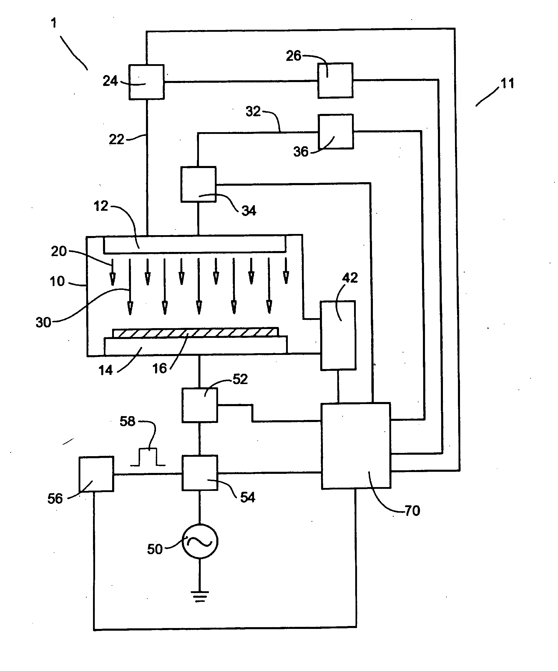
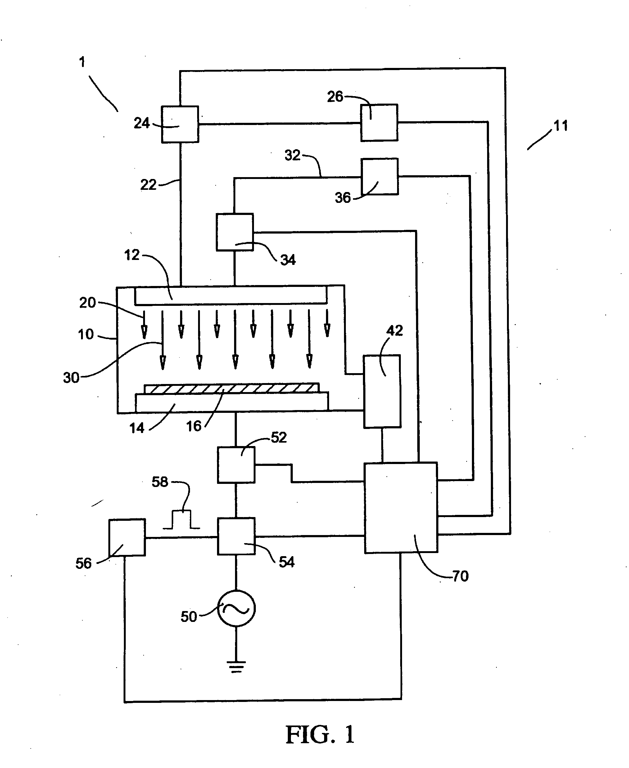
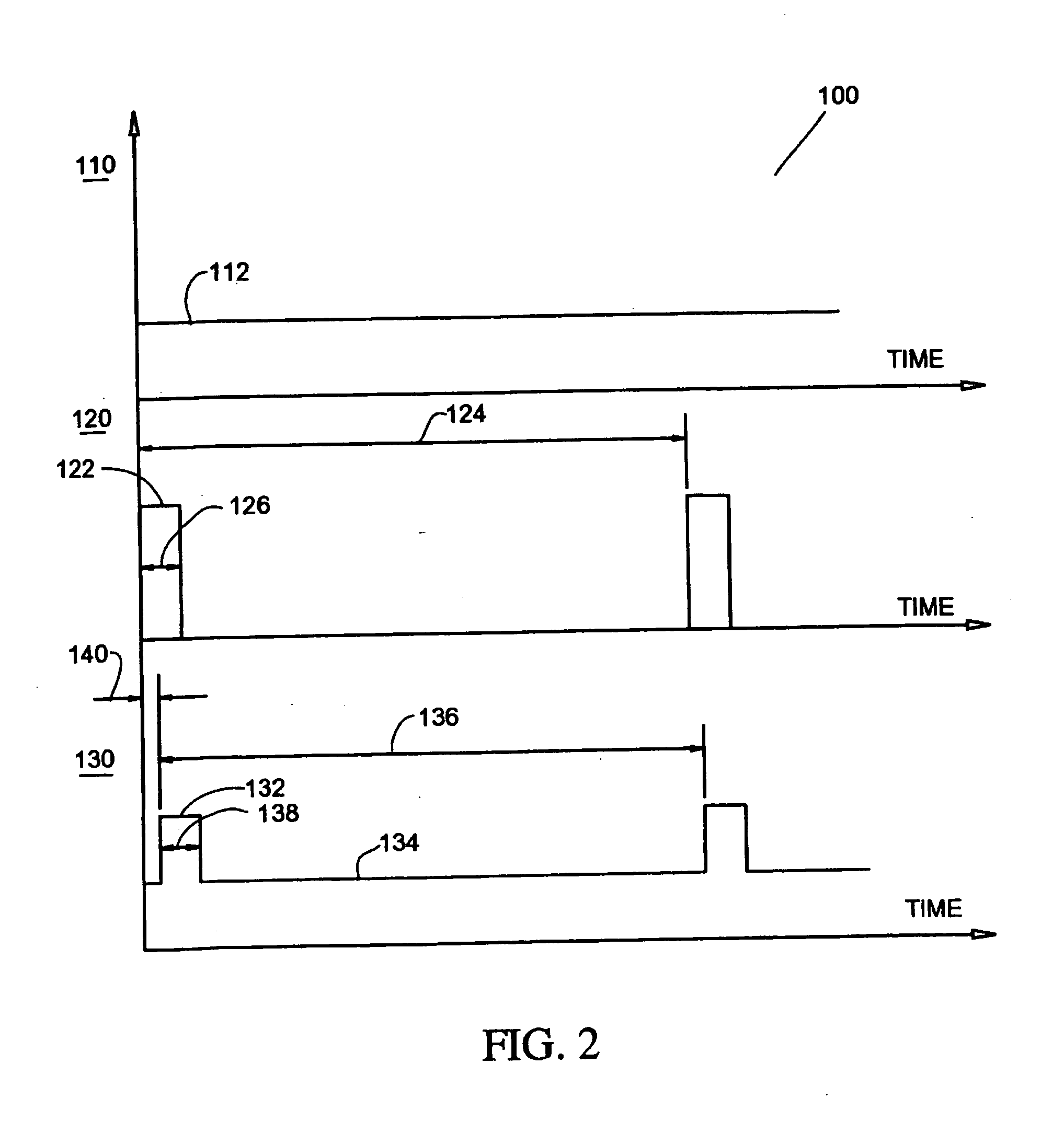
[0019] In order to improve deposition characteristics particularly in high aspect ratio features, the present invention improves a plasma processing system and method of operation to affect improvements in chemical transport local to an exposed substrate surface. The exposed substrate surface is exposed to material deposition steps, the combination of which serve to alter the material composition and / or topography of the exposed substrate surface. For example, deposition systems can include physical vapor deposition (PVD) systems, plasma-enhanced chemical vapor deposition (PECVD) systems, and atomic layer deposition (ALD) systems. For instance, in ALD processes, one or more gases can be pulsed with the flow of a continuous gas to form thin films of metal, metal nitride, metal oxide, nitrides, and oxides one monolayer at a time. One aspect of material deposition is chemical transport, which can be severely limited in high aspect ratio features due to the low densities associated with...


PUM

PropertyMeasurementUnit
Timeaaaaaaaaaa
Pressureaaaaaaaaaa
Poweraaaaaaaaaa

Abstract

A plasma processing system for performing atomic layer deposition (ALD) including a process chamber, a substrate holder provided within the process chamber, and a gas injection system configured to supply a first gas and a second gas to the process chamber. The system includes a controller that controls the gas injection system to continuously flow a first gas flow to the process chamber and to pulse a second gas flow to the process chamber at a first time. The controller pulses a RF power to the substrate holder at a second time. A method of operating a plasma processing system is provided that includes adjusting a background pressure in a process chamber, where the background pressure is established by flowing a first gas flow using a gas injection system, and igniting a processing plasma in the process chamber. The method includes pulsing a second gas flow using the gas injection system at a first time, and pulsing a RF power to a substrate holder at a second time.

Description

CROSS-REFERENCE TO RELATED APPLICATION [0001] This application is related to pending U.S. patent application Ser. No. 10 / 487,232, filed on Feb. 26, 2004, the entire contents of which are herein incorporated by reference.BACKGROUND OF THE INVENTION [0002] 1. Field of Invention [0003] The present invention relates to plasma processing and more particularly to a method for improved plasma processing. [0004] 2. Description of Related Art [0005] Typically, during materials processing, plasma is employed to facilitate the addition and removal of material films when fabricating composite material structures. For example, in semiconductor processing, a (dry) plasma etch process is utilized to remove or etch material along fine lines or within vias or contacts patterned on a silicon substrate. Alternatively, for example, a vapor deposition process is utilized to deposit material along fine lines or within vias or contacts on a silicon substrate. In the latter, vapor deposition processes incl...

Claims


Application Information

Patent Timeline
IPC IPC(8): H05H1/24H01J37/32C23C16/509
CPCC23C16/45525C23C16/45542C23C16/45544C23C16/5096H01J37/32082H01J37/32449H01J37/32935
Inventor STRANG, ERIC J.
Owner TOKYO ELECTRON LTD
Why Eureka
Try Eureka