

Electron beam writing method and lithography mask manufacturing method
a technology of lithography mask and writing method, which is applied in the direction of photomechanical equipment, instruments, originals for photomechanical treatment, etc., can solve the problems of inability to correct, inability to consider influences, and inability to carry out accurate corrections, etc., to achieve high precision, enhance in-plane uniformity, and prevent fluctuation of dimensional characteristics
- Summary
- Abstract
- Description
- Claims
- Application Information
AI Technical Summary
Benefits of technology
Problems solved by technology
Method used
Image

Examples
first embodiment
[First Embodiment]
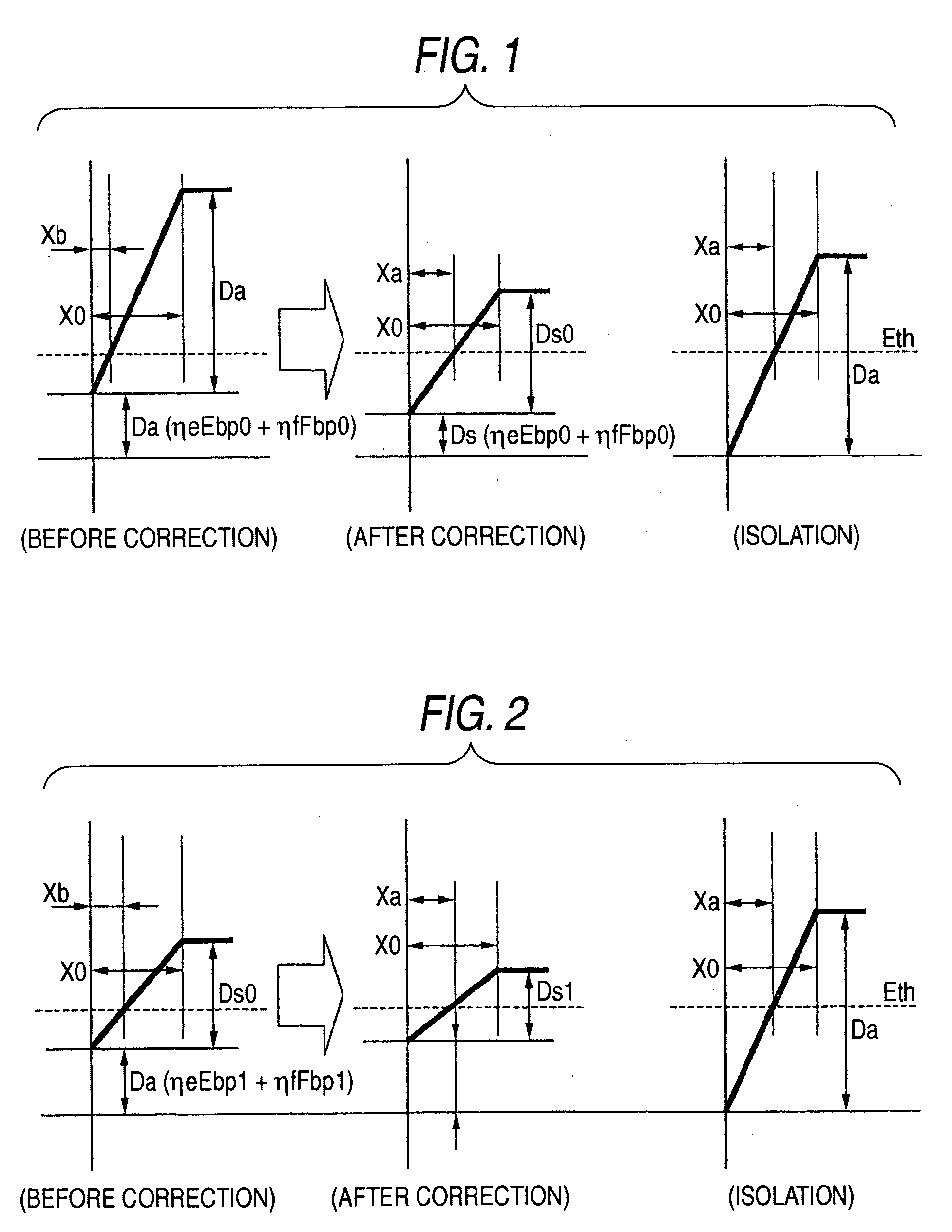
[0065] As a first embodiment of the electron beam writing method according to the invention, description will be given to the basic portion of the correction of the dimension of a writing pattern which unifies a proximity effect correction (PEC) and a Foggy effect correction. This relates to a multiple calculating technique which takes both the proximity effect and the Foggy effect into consideration.
[0066] In the following embodiment, description will be given on the assumption that a device for carrying out writing by an electron beam of 50 kV is used as a writing device.
[0067] A writing pattern to be a correcting object is divided by a rough mesh for a Foggy effect correction (which will be hereinafter referred to as a Foggy mesh and is 1 mm square (in all directions) in the embodiment) and a fine mesh for a proximity effect correction (which will be hereinafter referred to as a proximity effect correcting mesh and is 0.5 μm square (in all directions) in the e...
second embodiment
[Advantage of Second Embodiment]
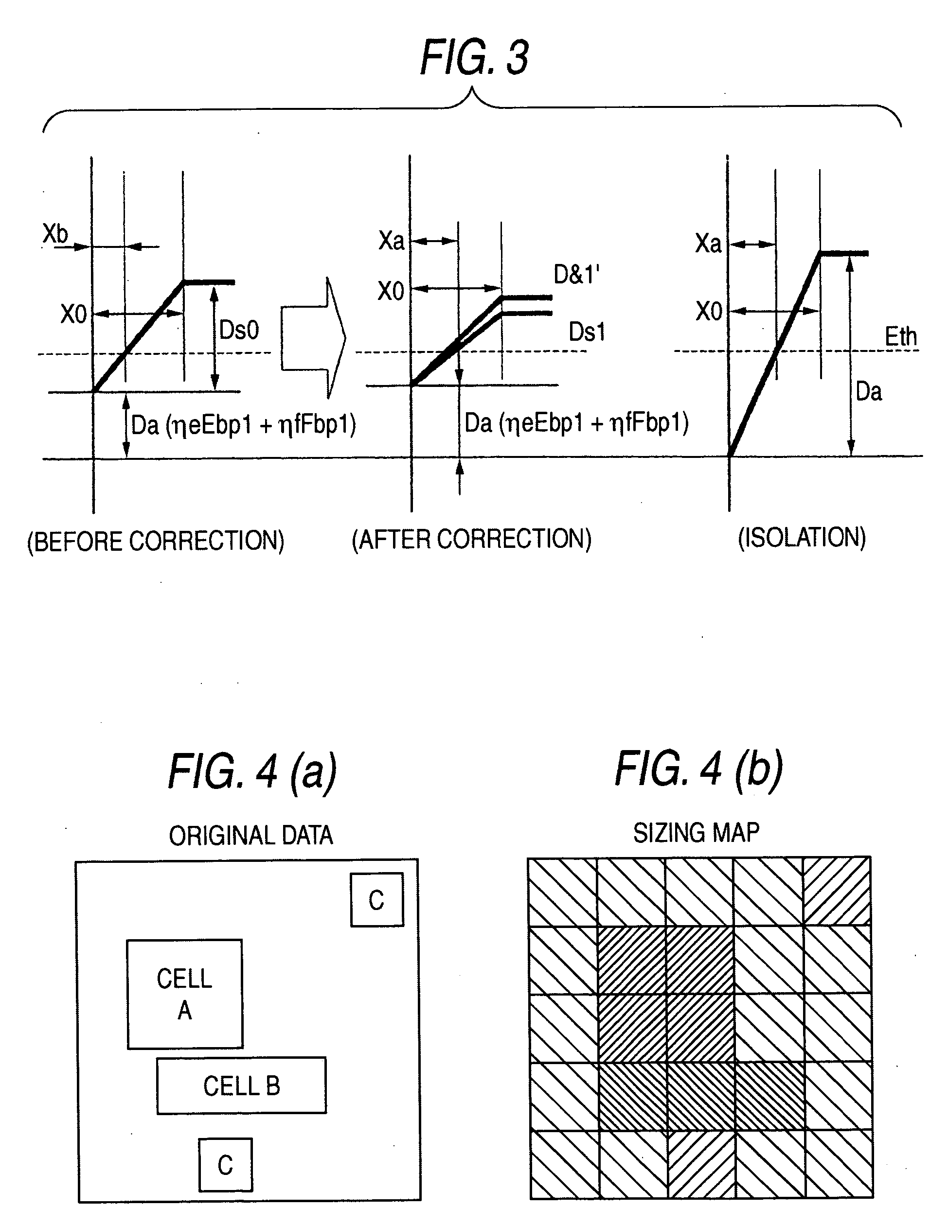
[0102] In the embodiment, it is possible to carry out a correction with high precision in consideration of both a Foggy effect and a proximity effect and the convergence of a solution is more excellent than that in the first embodiment. In order to obtain precision to an almost equal extent, it is sufficient that the number of times of a recalculation is approximately ⅓ of that in the first embodiment.
[Third Embodiment]
[0103] A third embodiment provides a method of incorporating the correction of a developing uniformity on the assumption of the use of the first embodiment or the second embodiment. Description will be given on the assumption that a device for carrying out writing by an electron beam of 50 kV is used as a writing device.
[0104] First of all, a writing pattern to be a correcting object is divided by a Foggy mesh (1 mm square (in all directions) in the embodiment) and a proximity effect correcting mesh (0.5 μm square (in all directions)...
third embodiment
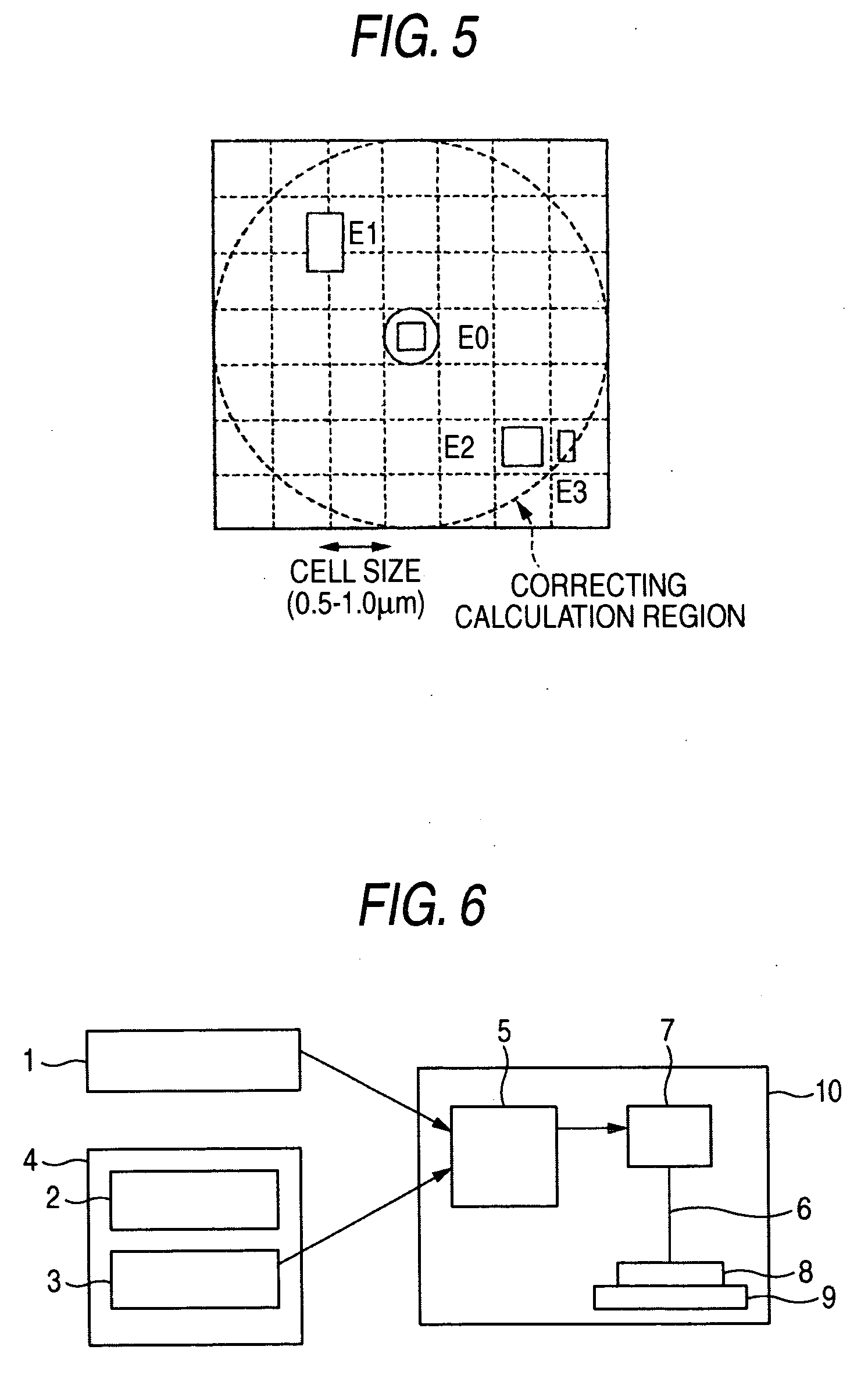
[Advantage of Third Embodiment]
[0122] In the embodiment, it is possible to carry out a correction with high precision in consideration of both the Foggy effect and the proximity effect, and furthermore, to prevent a fluctuation in a dimensional characteristic based on the density of a pattern which is changed by only the in-plane correction of a sensitivity. Accordingly, it is possible to enhance an in-plane uniformity in a resist stage.
[Fourth Embodiment]
[0123] A fourth embodiment provides a method of incorporating the correction of an etching uniformity according to the third embodiment on the assumption that a writing device capable of inputting an exposure parameter every Foggy mesh is used.
[0124] The in-plane distribution (nonuniformity) of etching can be represented as the in-plane distribution of an etching critical dimension loss in a state in which the in-plane distribution of a resist can be disregarded, that is, the third embodiment is carried out.
[0125] In order to o...
PUM
 Abstract
Description
Claims
Application Information