Process for producing nitride semiconductor light-emitting device

Inactive Publication Date: 2005-10-06
SAMSUNG ELECTRONICS CO LTD
View PDF7 Cites 11 Cited by
  • Summary
  • Abstract
  • Description
  • Claims
  • Application Information

AI Technical Summary

Benefits of technology

[0014] Therefore, the present invention has been made in view of the above problems, and it is an object of the present invention to provide a process for producing a nitride semiconductor light-emitting device having an n-type nitride semiconducto

Problems solved by technology

These substrates for growth of nitride single crystals are electrically insulative, and thereby, electrodes cannot be mounted on the back surface of the substrate unlike conventional light-emitting devices.
However, the transparent electrode 18 made of Ni/Au has a transmissivity of only about 60%, suffering from great loss of light due to absorption.
Further, a complex process is required to add a

Method used


Image

  • Process for producing nitride semiconductor light-emitting device
  • Process for producing nitride semiconductor light-emitting device
  • Process for producing nitride semiconductor light-emitting device

Examples


Example

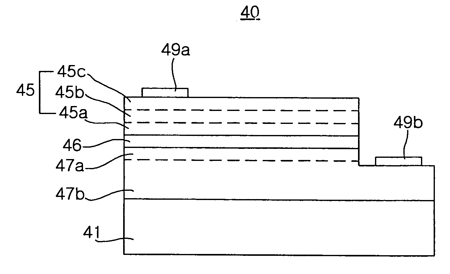
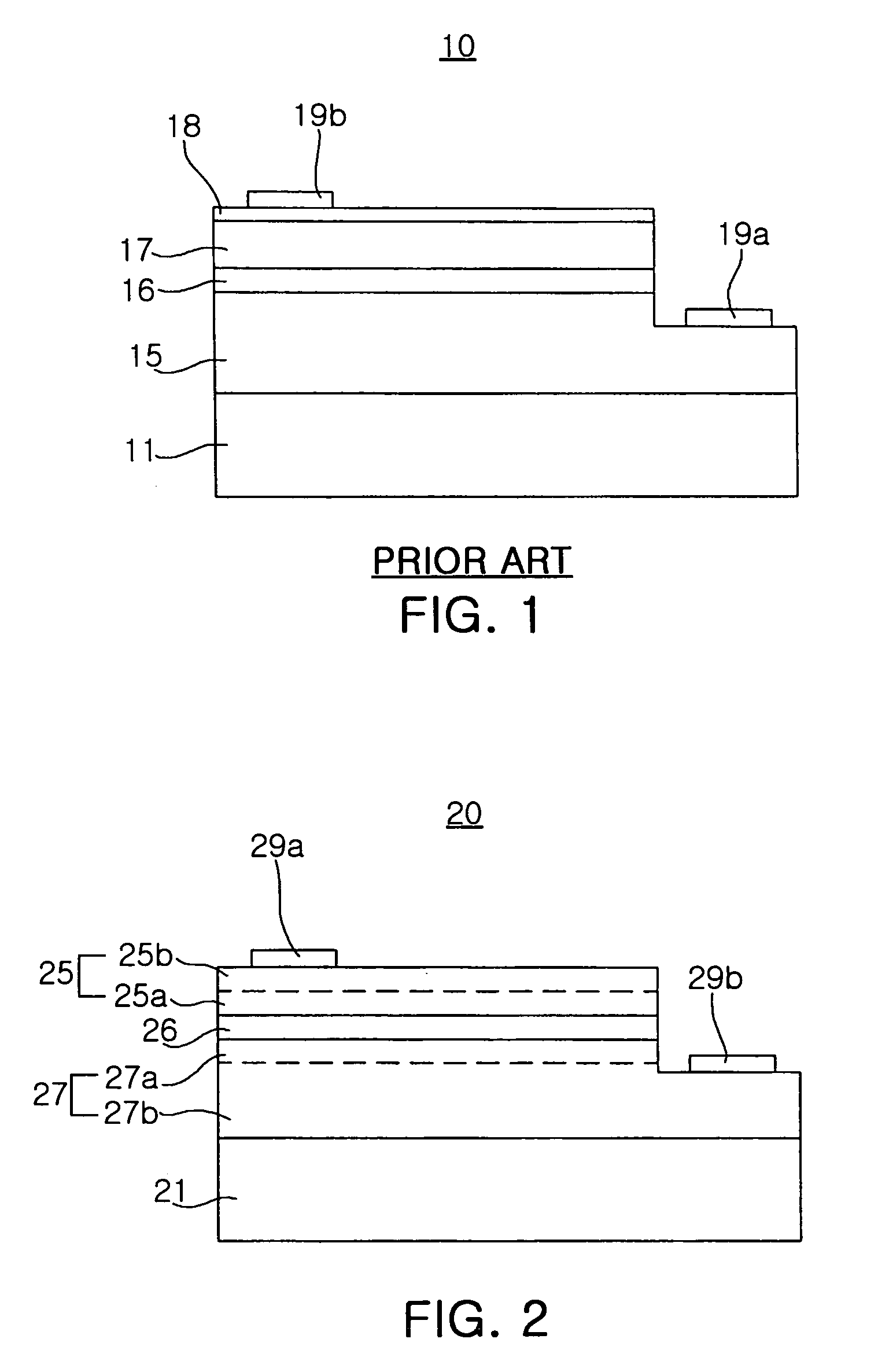
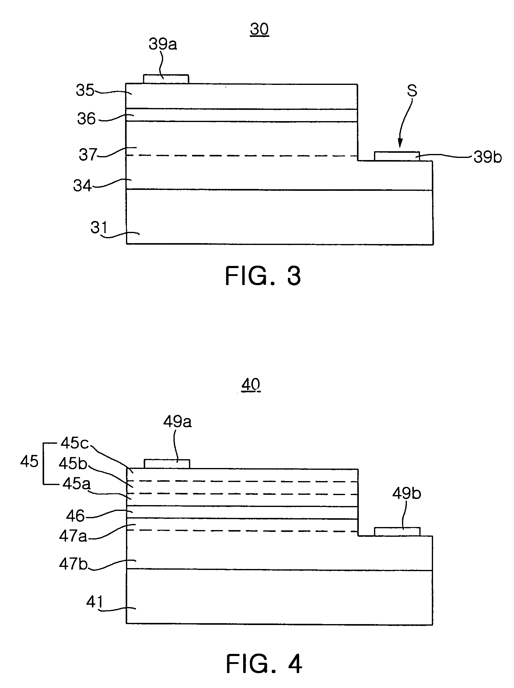
[0040] Preferred embodiments of the present invention will now be described in detail with reference to the annexed drawings. FIG. 2 is a cross-sectional side view of a nitride semiconductor light-emitting device 20 according to one embodiment of the present invention.

[0041] As shown in FIG. 2, the nitride semiconductor light-emitting device 20 includes a sapphire substrate 21, and a p-type nitride semiconductor layer 27, an active layer 26 and an n-type nitride semiconductor layer 25, these layers being formed sequentially on the sapphire substrate 21. Further, in order to improve a lattice matching of the p-type nitride semiconductor layer 27 with the sapphire substrate 21, a buffer layer may be formed thereon prior to growth of the p-type nitride semiconductor layer 27. As the buffer layer, a low temperature nucleus-growth layer made of a formula AlxInyGa1−(x+y)N (0≦x, y≦1) material may be used.

[0042] Referring now to FIG. 2, a process for producing the nitride semiconductor li...


PUM

PropertyMeasurementUnit
Temperatureaaaaaaaaaa
Electrical conductoraaaaaaaaaa
Semiconductor propertiesaaaaaaaaaa

Abstract

A process for producing a nitride semiconductor light-emitting device includes the steps of preparing a substrate, growing a p-type nitride semiconductor layer on the substrate by the MOCVD process using hydrazine-based gas as a nitrogen precursor and N2 gas as a carrier gas, forming an active layer on the p-type nitride semiconductor layer, forming an n-type conductive nitride semiconductor layer on the active layer, and forming p- and n-electrodes in electrical connection with the p- and n-type nitride semiconductors, respectively.

Description

BACKGROUND OF THE INVENTION [0001] 1. Field of the Invention [0002] The present invention relates to a process for producing a nitride semiconductor light-emitting device, and more particularly to a process for producing a nitride semiconductor light-emitting device having a novel structure in which a transparent electrode layer for improving contact resistance on a p-electrode may be eliminated. [0003] 2. Description of the Related Art [0004] A nitride semiconductor light-emitting device is a high output power optical device that produces short wavelength light such as blue, green light, or the like, thus enabling it to produce a variety of colors, and attracts a great deal of attention in the related technical art [0005] A constituent material of the nitride semiconductor light-emitting device is semiconductor single crystals of a composition formula AlxInyGa(1−x−y)N (0≦x,y,x+y≦1) Nitride semiconductor single crystals may be grown on substrates such as sapphire or SiC by using cry...

Claims


Application Information

Patent Timeline
IPC IPC(8): H01L21/00H01L21/20H01L21/205H01L21/28H01L21/3205H01L29/22H01L29/24H01L33/00
CPCH01L21/0237H01L21/0242H01L21/02458H01L21/0254H01L21/02579H01L21/0262H01L33/007E02D5/38E02D27/14E02D2250/0023E02D2300/0006E02D2600/20E02D2600/30
Inventor CHO, DONG HYUNKOIKE, MASAYOSHIHAHM, HUN JOO
Owner SAMSUNG ELECTRONICS CO LTD
Why Eureka
Try Eureka