Method for modifying existing micro-and nano-structures using a near-field scanning optical microscope

a scanning optical microscope and micro-structure technology, applied in the direction of scanning probe techniques, instruments, manufacturing tools, etc., can solve the problems of complex lithographic methods, high-cost techniques usually require stringent environmental conditions, and complicated manufacture of materials

Inactive Publication Date: 2005-10-06
PANASONIC CORP
View PDF10 Cites 19 Cited by
  • Summary
  • Abstract
  • Description
  • Claims
  • Application Information

AI Technical Summary

Problems solved by technology

The feature sizes used to form photonic crystals and the precise alignment requirements of these features complicate manufacture of these materials.
One challenge in producing micro-circuitry is preventing shorts between components and nano-wires which are located ever closer together.
These high-cost techniques usually require stringent environmental conditions, such as high vacuum or clean room condition.
All the lithographic methods require a series of complicated procedures, which involve generating multiple masks and using photoresist.
Still alignment of a laser beam to nanostructures on existing microstructures is a difficult issue.
These high-cost techniques usually require stringent environmental conditions, such as high vacuum or clean room condition.
All the lithographic methods require a series of complicated procedures, which involve generating multiple masks and using photoresist.

Method used


Image

  • Method for modifying existing micro-and nano-structures using a near-field scanning optical microscope
  • Method for modifying existing micro-and nano-structures using a near-field scanning optical microscope
  • Method for modifying existing micro-and nano-structures using a near-field scanning optical microscope

Examples


Embodiment Construction

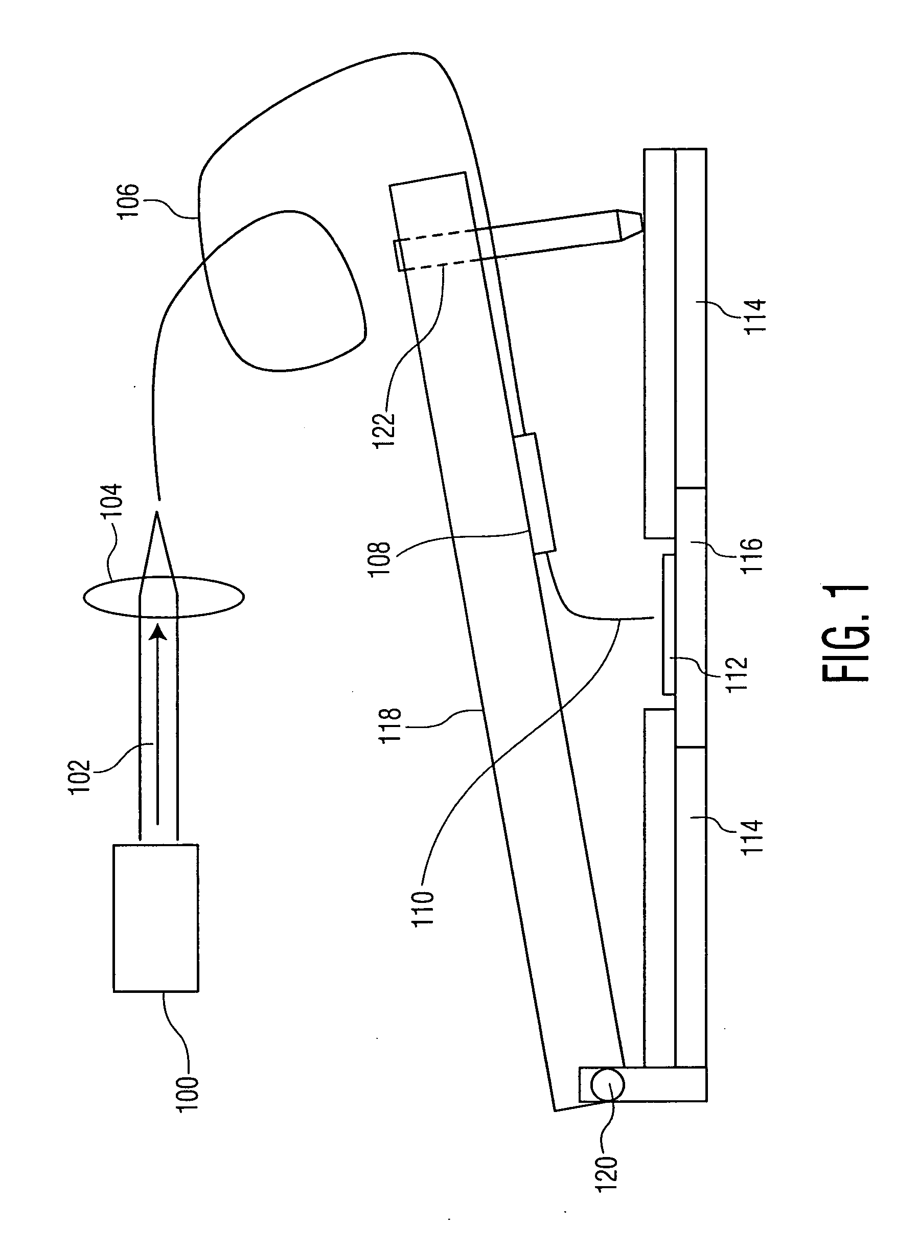
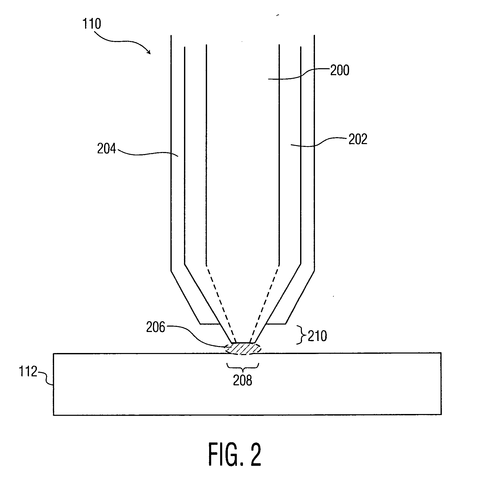
[0030] NSOMs use many of the same principles as atomic force microscopes (AFMs) to accurately profile surfaces. Laser micromachining of these surfaces using near-field radiation from an NSOM probe tip may provide a number of advantages compared to using non-near-field radiation and free space optics. The advantages may include precise positioning control of the NSOM probe tip and a reduced minimum feature size. The precise motion stages used in NSOM devices may be used to provide precise horizontal (X and Y) and vertical (Z) positioning control. Additionally, the ability of an NSOM to profile a surface allows for the accurate vertical positioning of the probe tip desired to couple significant near-field radiation to the surface.

[0031] The minimal feature size that may be machined with an exemplary NSOM laser machining system of the present invention using near-field radiation is determined by the size of the NSOM probe tip, rather than by the wavelength of the laser light used to g...


PUM

PropertyMeasurementUnit
distanceaaaaaaaaaa
distanceaaaaaaaaaa
pitch sizeaaaaaaaaaa

Abstract

A method for manufacturing a microstructure, which includes at least one fine feature on an existing feature, using an NSOM laser micromachining system. A microstructure device preform is provided. A portion of its top surface is profiled with the NSOM to produce a topographical image. This profiled portion is selected to include the existing feature. An image coordinate system is defined for the profiled portion of top surface based on the topographical image. Coordinates of a reference point and the orientation of the existing feature in the image coordinate system are determined using the topographical image. The probe tip of the NSOM is aligned over a portion of the existing feature using the determined coordinates of the reference point and the orientation of the existing feature. The top surface of the microstructure device preform is machined with the micro-machining laser to form the fine feature(s) on the existing feature.

Description

FIELD OF THE INVENTION [0001] The present invention concerns an apparatus and method for laser machining of existing features on existing microstructures, including nanostructures, using a near-field scanning optical microscope (NSOM). This method may also allow mass customization or repair of generic electronic and mechanical microstructures. BACKGROUND OF THE INVENTION [0002] As products get smaller and smaller, there is increased demand for micro-electrical-mechanical systems (MEMS), micro-optical devices and photonic crystals. With this demand, there is an associated increased interest in micro- and nano-machining. Numerous applications exist for MEMS. As a breakthrough technology, allowing unparalleled synergy between previously unrelated fields such as biology and microelectronics, new MEMS applications are emerging at a rapid pace, expanding beyond those currently identified or known. Additional applications in quantum electric devices, micro-optical devices and photonic crys...

Claims


Application Information

Patent Timeline
Patent Type & Authority Applications(United States)
IPC IPC(8): B23K26/06B81C1/00B81C99/00G01Q10/04G01Q40/00G01Q60/18G01Q60/22G01Q80/00
CPCB81C1/00492B81C99/0065B82Y20/00B82Y30/00G01Q80/00G01Q60/22Y10S977/851
Inventor LI, MINGISHIZUKA, MAKOTOCHENG, CHEN-HSIUNG
Owner PANASONIC CORP
Why Eureka
Try Eureka