Lead frame, method of manufacturing the same, semiconductor device using lead frame and method of manufacturing semiconductor device

a manufacturing method and lead frame technology, applied in the direction of valve housings, multiple-way valves, mechanical devices, etc., can solve the problems of increasing the man-hour in the manufacturing process, imperfect contact, etc., and achieves no deformation, stable external terminal structure, and high reliability

Inactive Publication Date: 2005-10-13
COLLABO INNOVATIONS INC
View PDF8 Cites 9 Cited by
  • Summary
  • Abstract
  • Description
  • Claims
  • Application Information

AI Technical Summary

Benefits of technology

[0077] According to the above constitution, in the case of mounting a semiconductor chip, the lead portion is fixed to the lead frame body. Therefore, a positional deviation is not caused and bonding can be performed with high reliability. After the lead portion has been positively fixed by means of resin sealing, the lead frame body is removed from the reverse side. Therefore, no deformation is caused in the semiconductor device.
[0078] Since the lead portion is formed protruding from the groove portion, the lead portion protruding from the sealing resin is not subjected to a plating process after resin sealing, and a stable external terminal structure can be formed. Therefore, the semiconductor device can be assembled to a printed board without the occurrence of an imperfect contact.
[0079] A highly reliable thin semiconductor device can be easily provided.
[0080] After the completion of resin sealing, dicing is conducted so that the semiconductor device can be divided into individual pieces. Since it is possible to make the lead portion not exist in the dicing region, and it is unnecessary that a cutting blade cuts the lead portion at the time of dicing. Therefore, abrasion of the cutting blade can be reduced and the blade life can be extended.
[0081] In addition to that, the profile of the cross-section of the lead portion can be freely designed according to the profile of the cross-section of the groove portion. Therefore, a highly dense, accurate semiconductor device can be easily formed.

Problems solved by technology

However, on the contact face of the resin sealing type semiconductor device with the printed board, that is, on the reverse side of the semiconductor integrated circuit device, since the resin face and the lead terminals, which become the external terminals, are on the same plane, even when a small deviation of the size is caused, it is impossible to positively connect with the circuit pattern on the printed board, which could cause an imperfect contact.
In order to protrude the lead terminals, it is necessary to provide a plating process in which the bumps (the protruding portions) are formed after the completion of dicing, which increases the man-hour in the manufacturing process.

Method used


Image

  • Lead frame, method of manufacturing the same, semiconductor device using lead frame and method of manufacturing semiconductor device
  • Lead frame, method of manufacturing the same, semiconductor device using lead frame and method of manufacturing semiconductor device
  • Lead frame, method of manufacturing the same, semiconductor device using lead frame and method of manufacturing semiconductor device

Examples


first embodiment

[0103] First Embodiment

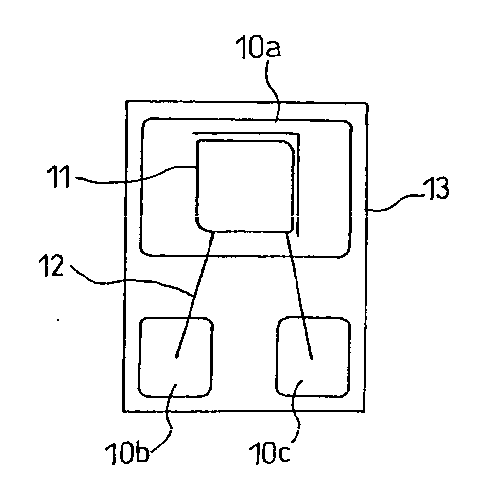
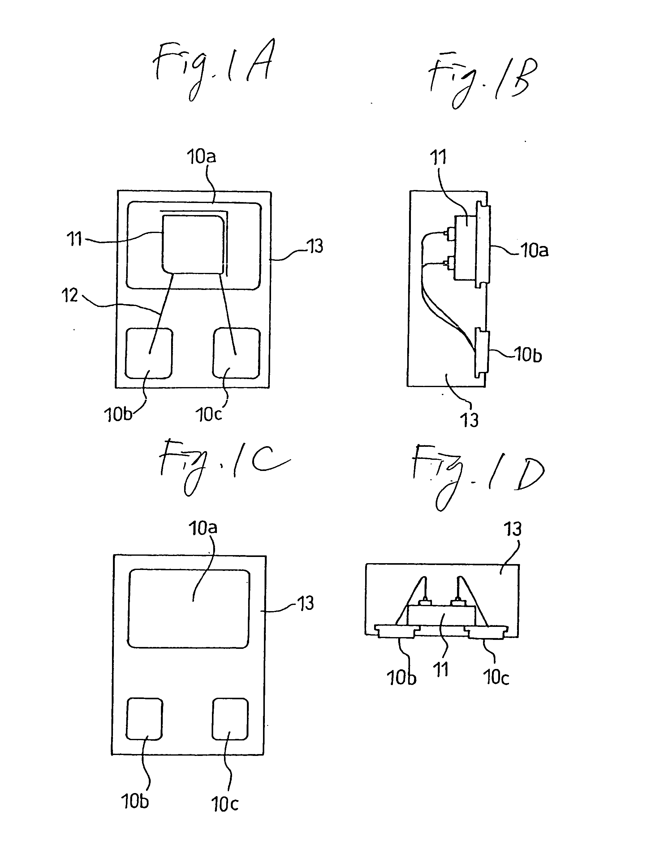
[0104]FIGS. 1A to 1C are respectively an upper view, a cross-sectional view taken on line A-A, a lower view and a cross-sectional view taken on line B-B showing a semiconductor device of the first embodiment of the present invention. As shown in the drawings, this semiconductor device is a face assembly type semiconductor device, which is formed as follows. The semiconductor chip 11 composing a bipolar transistor is set on the die pad 10a, and the pad connected to the collector and the pad connected to the emitter are respectively electrically connected to the lead terminals 10b, 10c via the bonding wires 12 and sealed with resin. From the reverse face of this sealing resin, the die pad 10a composing the base terminal and the lead terminals 10b, 10c composing the emitter terminal and the collector terminal are somewhat protruded, so that a face assembly type semiconductor device can be formed.

[0105] The die pad and the lead terminal comprise a three layer str...

second embodiment

[0144] Second Embodiment

[0145] Next, the second embodiment of the present invention will be explained below.

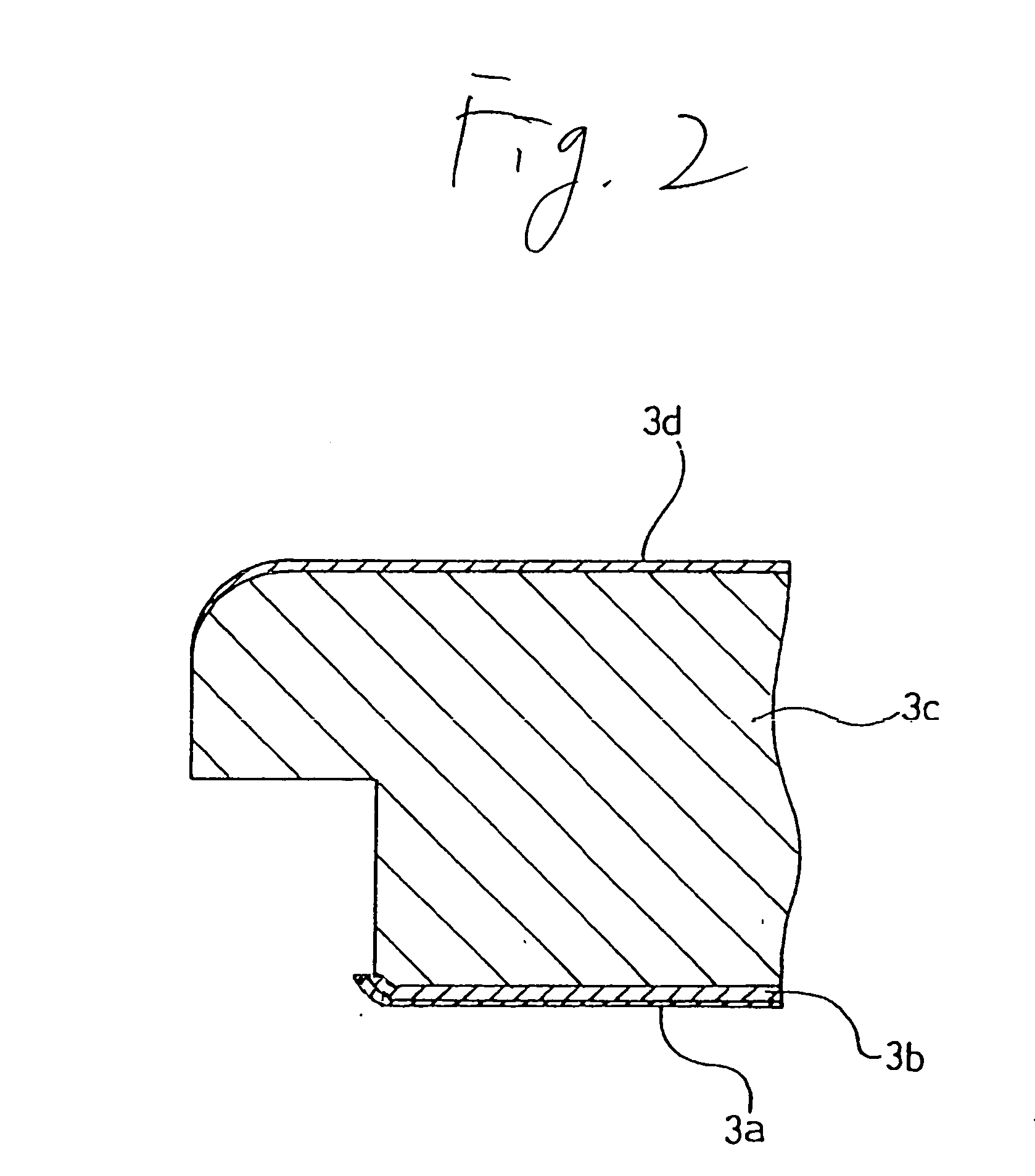
[0146] In the semiconductor device of this embodiment, the external terminal structure is formed as follows. As show in FIG. 10, after the first conductor layers 3c, 3d have been formed in such a manner that the first conductor layers 3c, 3d rise from the inside of the groove portion to the flat portion, the second and the third conductor layer are laminated on each other so that an end edge portion of the first conductor layer 3b can be left, and the entire surface of the external terminal composes the external terminal structure covered with the first conductor layer.

[0147] In this case, there is provided a nickel layer, which is used as the barrier layer 3a, on the outer layer of the first conductor layer 3b.

[0148] As described above, the conductor layer is formed in such a manner that the circumferential edge of the groove portion is exposed and made to rise from the in...


PUM

PropertyMeasurementUnit
thicknessaaaaaaaaaa
depthaaaaaaaaaa
depthaaaaaaaaaa

Abstract

There is provided a lead frame which comprises: a lead frame body comprising a sheet-shaped body made of metal; a groove portion for forming a lead which is formed by a predetermined depth in a lead forming region on a surface of the lead frame body; and a lead portion formed so that the lead portion can protrude from the groove portion onto the surface of the lead frame body, the lead portion being made of material different from material of the lead frame body. A thin type semiconductor device is provided in which the above lead frame is used and after a chip is mounted, the lead frame body is removed by means of etching.

Description

[0001] The present application is based on Japanese Patent Application No. 2003-008349, which is incorporated herein by reference. BACKGROUND OF THE INVENTION [0002] 1. Field of the Invention [0003] The present invention relates to a lead frame, a method of manufacturing the lead frame, a semiconductor device using the lead frame and a method of manufacturing the semiconductor device. More particularly, the present invention relates to the formation of an external terminal of a resin sealing type semiconductor device. [0004] 2. Description of the Related Art [0005] Recently, electronic equipment such as a personal computer and cellular phone has been downsized. According to this tendency of downsizing electronic equipment, electronic parts are highly densely assembled. Therefore, in the field of a semiconductor device such as a diode and transistor, in order to reduce the assembling area, a face assembly type semiconductor device is widely used. [0006] In this face assembly type sem...

Claims


Application Information

Patent Timeline
Patent Type & Authority Applications(United States)
IPC IPC(8): H01L23/48C25D1/00H01L21/56H01L21/68H01L23/31H01L23/495H01L23/50
CPCH01L21/561H01L21/565H01L21/568H01L23/3107H01L23/49562H01L23/49582H01L24/48H01L24/97H01L2224/05644H01L2224/32245H01L2224/48091H01L2224/48095H01L2224/48247H01L2224/48465H01L2224/73265H01L2224/83001H01L2224/85001H01L2224/85399H01L2224/97H01L2924/01004H01L2924/01005H01L2924/01006H01L2924/01014H01L2924/01015H01L2924/0102H01L2924/01022H01L2924/01027H01L2924/01028H01L2924/01029H01L2924/01032H01L2924/01033H01L2924/01046H01L2924/01047H01L2924/0105H01L2924/01074H01L2924/01078H01L2924/01079H01L2924/01082H01L2924/01322H01L2924/014H01L2924/14H01L2924/18301H01L2924/19043H01L2924/00014H01L24/32H01L2924/0132H01L2224/83805H01L2924/01019H01L2924/00H01L2224/45099H01L2924/12041C25D1/003H01L2224/85444H01L2924/00012H01L2924/1305H01L21/6835H01L2221/68345H01L2221/68381H01L2924/181H01L24/73H01L2224/29099F16K11/085F16K27/065
Inventor KOBAYASHI, TAKESHISUGOH, HISAO
Owner COLLABO INNOVATIONS INC
Why Eureka
Try Eureka