Electro-optical device and method of manufacturing the same

a technology of optical devices and optical components, applied in the field of optical components, can solve the problems of reducing aperture ratio, deteriorating display quality, increasing manufacturing cost, etc., and achieve the effect of low cost and simple manufacturing process

Inactive Publication Date: 2005-10-20
SEIKO EPSON CORP
View PDF4 Cites 46 Cited by
  • Summary
  • Abstract
  • Description
  • Claims
  • Application Information

AI Technical Summary

Benefits of technology

[0026] The electro-optical device may be, for example, a liquid crystal display device having a pair of substrate with liquid crystal, which is electro-optical material, interposed therebetween. On one of the substrates, there are provided an electrode layer, a group of electrodes provided on the electrode layer with an insulating layer interposed therebetween, non-linear resistance elements, one end of each of the non-linear resistance elements being connected to the respective one of the group of electrodes, and pixel electrodes provided on the electrode layer with the insulating layer interposed therebetween, each pixel electrode being connected to the other end of each of the non-linear resistance elements. Therefore, a so-called transverse electric field is generated in a substantially parallel direction to a flat surface of the substrate by conducting between the electrode layer and the pixel electrodes, and thus alignment of electro-optical material such as liquid crystal is controlled by the transverse electric field. Further, since the non-linear resistance elements have a so-called TFD (MIM) structure made of metal-insulating layer-metal, the manufacturing process is simple. Therefore, the transverse electric field mode display device can be manufactured at low cost.

Problems solved by technology

However, since, in order to form a TFT element, it is necessary to perform exposure, development and etching processes in a number of times, the manufacturing process becomes complicated to consequently increase the manufacturing cost.
However, display quality deteriorates because of the occurrence of transverse irregularity or vertical crosstalk on display image.
However, such a shield structure results in a decreasing aperture ratio.

Method used


Image

  • Electro-optical device and method of manufacturing the same
  • Electro-optical device and method of manufacturing the same
  • Electro-optical device and method of manufacturing the same

Examples


first exemplary embodiment

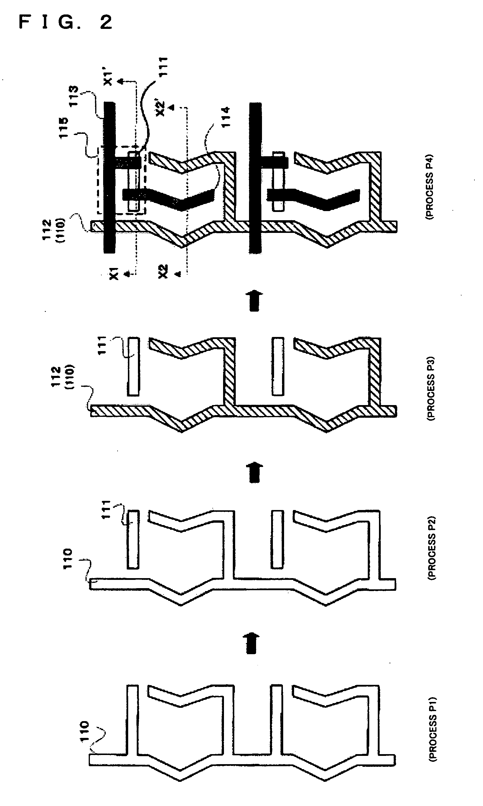
[0065] A first exemplary embodiment comprises an IPS mode electrode structure 1. FIG. 2 is a schematic plan view showing a manufacturing process of a portion of an electrode structure according to the first exemplary embodiment, and FIGS. 3A-D and 4A-D are schematic partial cross-sectional views thereof. Moreover, FIG. 2 shows an area corresponding to two pixels vertically disposed. FIG. 3 is a schematic cross-sectional view taken along line X1-X1′ of FIG. 2, and FIG. 4 is a schematic cross-sectional view taken along line X2-X2′ of FIG. 2.

[0066] According to a method of manufacturing the electrode structure 1, as shown in FIGS. 2 to 4, a signal electrode 110 made of tantalum (Ta) is formed on the transparent substrate 11 in a process P1. Specifically, tantalum is formed on the transparent substrate 11 made of glass by a sputtering process and then is shaped by a photolithography process as shown in FIGS. 2 to 4. Then, the shaped tantalum is oxidized by anode oxidization to form an ...

second exemplary embodiment

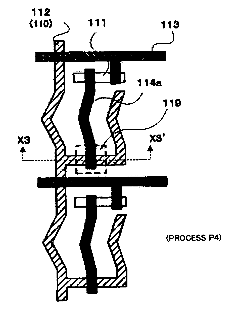
[0072] Next, a second exemplary embodiment will be now described. FIG. 5A is a schematic plan view showing an electrode structure 1 according to the second exemplary embodiment, and FIG. 5B is a schematic sectional view taken along line X3-X3′ of FIG. 5A. As compared with FIG. 2, the electrode structure 1 of the second exemplary embodiment is fundamentally the same as that of the first exemplary embodiment. However, the second exemplary embodiment is different from the first exemplary embodiment in that a storage capacitor is formed by crossing the pixel electrode 114a and the signal electrode 110 in an area 119 indicated by a broken line.

[0073] Assuming that a capacitor of the TFD element portion 115 is CTFD and the storage capacitor of the area 119 is CPIX, it is possible to obtain a satisfactory contrast by setting the ratio of CPIX / CTFD to be about 6 through 12.

[0074] A specific manufacturing method is almost the same as the manufacturing method of the first exemplary embodime...

third exemplary embodiment

[0075] Next, a third exemplary embodiment will be now described. FIG. 6A is a schematic plan view showing the electrode structure 1 according to a first exemplary example of a third exemplary embodiment, and FIG. 6B is a schematic sectional view taken along line X4-X4′ of FIG. 6A. The electrode structure 1 according to the first exemplary example of the third exemplary embodiment is fundamentally the same or similar as that of the first exemplary embodiment. However, in the third exemplary embodiment, as shown in FIG. 6A, a chromium electrode 116 or 117 is further formed on the signal electrode 110, thereby reducing resistance of the signal electrode 110. As described in the first exemplary embodiment, in a process P3, an oxide film is formed as an insulating layer 112 on a surface of the signal electrode 110 by anode-oxidizing the signal electrode 110. As a result, the signal electrode 110 decreases in film thickness by the oxide film 112, thereby increasing resistance. Thus, in th...


PUM

PropertyMeasurementUnit
electro-opticalaaaaaaaaaa
non-linear resistanceaaaaaaaaaa
insulatingaaaaaaaaaa

Abstract

To simplify a manufacturing process of a transverse electric field mode liquid crystal display device by using a non-linear resistance element such as a TFD (Thin Film Diode) as a switching element. In a liquid crystal display device having a pair of substrates with liquid crystal interposed therebetween, one of the substrates consists of an electrode substrate. On the electrode substrate, there are provided a first group of electrodes, a second group of electrodes crossing the first group of electrodes with an insulating layer interposed therebetween, non-linear resistance elements, one end of each of the non-linear resistance elements being connected to the respective one of the second group of electrodes, and pixel electrodes opposing the first group of electrodes, each pixel electrode being connected to the other end of each of the non-linear resistance elements. Since the non-linear resistance elements have a so-called TFD (MIM) structure made of metal-insulating layer-metal, the manufacturing process is simple. Therefore, it is possible to manufacture the transverse electric field mode display device at low cost.

Description

BACKGROUND OF THE INVENTION [0001] 1. Field of Invention [0002] The present invention relates to an electro-optical device, such as a liquid crystal display device. The present invention also relates to a transverse electric field mode liquid crystal display device. [0003] 2. Description of Related Art [0004] In related art TN (Twisted Nematic) mode liquid crystal display devices, alignment of liquid crystal molecules is controlled by sealing liquid crystal between two transparent substrates and applying an electric field in a vertical direction to the substrate via a transparent electrode provided on each of the substrates. Related art document Japanese Unexamined Patent Application Publication No. 2000-162602 discloses that an electric field is applied to liquid crystal in a nearly parallel direction to the substrate. This is referred to as a transverse electric field mode or an IPS (In-Plane Switching) mode. [0005] In the related art liquid crystal display device, a TFT (Thin Fil...

Claims


Application Information

Patent Timeline
Patent Type & Authority Applications(United States)
IPC IPC(8): G02F1/133G02F1/1365G02F1/1343G02F1/136G09F9/30H01L49/02
CPCG02F1/1365G02F1/134363G02F1/1343
Inventor YAMAZAKI, KATSUNORIOKAMOTO, EIJIMAEDA, TSUYOSHIKAMIJO, KIMITAKANAGANO, DAISUKESEKI, TAKUMIINOUE, AKIRA
Owner SEIKO EPSON CORP
Why Eureka
Try Eureka