

Electronic circuit device having silicon substrate
a technology of electronic circuit device and silicon substrate, which is applied in the direction of fluid speed measurement, instrumentation, and the details of the semiconductor/solid-state device, can solve the problems of large mounting area and volume, and achieve the effect of reducing size and weigh
- Summary
- Abstract
- Description
- Claims
- Application Information
AI Technical Summary
Benefits of technology
Problems solved by technology
Method used
Image

Examples
embodiment 1
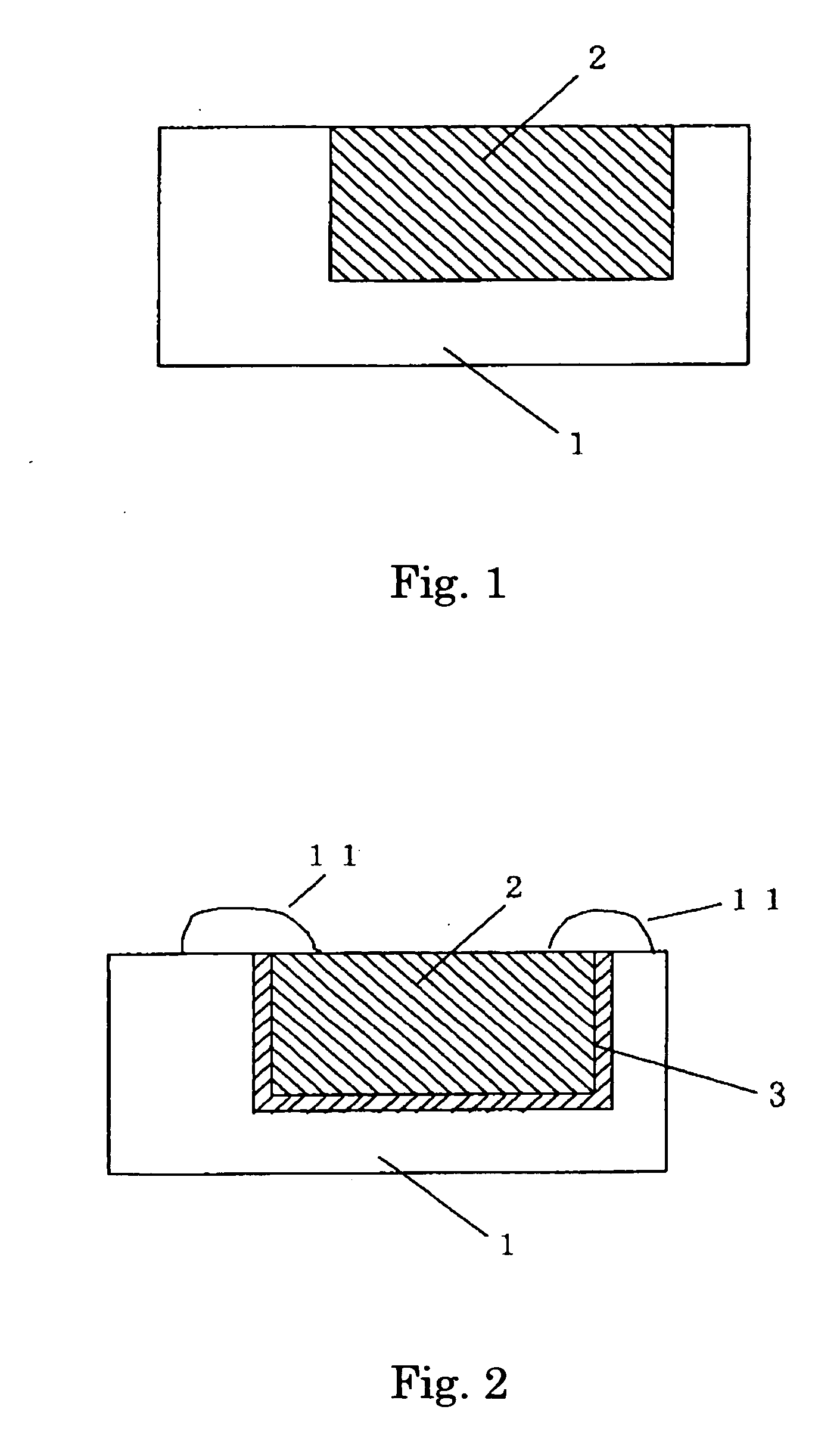
[0038] Hereinafter, description will be made of embodiments of the present invention with reference to the accompanying drawings. FIG. 1 is a sectional view of an electronic circuit device having a silicon substrate according to Embodiment 1 of the present invention.
[0039] A silicon substrate 1 has a front surface and a back surface. The upper side of FIG. 1 corresponds to the front surface, and the lower side thereof corresponds to the back surface. On the front surface of the silicon substrate 1, elements, which are not shown in the figure, such as a transistor, a resistor, and a capacitor are formed by using a silicon planar process, which is a technology of directly forming an integrated circuit on a semiconductor substrate adopting methods of deposition, etching, doping, heat treatment, and the like.
[0040] Further, a recess is formed on the front surface of the silicon substrate 1 by anisotropic silicon dry etching such as DRIE (Deep Reactive Ion Etching) or anisotropic wet e...
embodiment 2
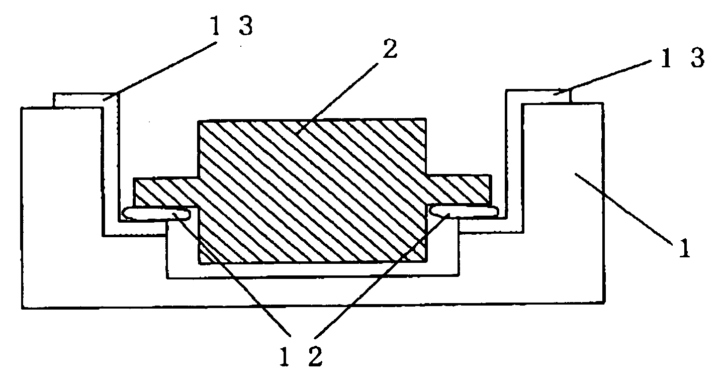
[0047]FIG. 4 is a sectional view of an electronic circuit device having a silicon substrate according to Embodiment 2 of the present invention. The silicon substrate 1 has a front surface and a back surface. The upper side of FIG. 4 corresponds to the front surface, and the lower side thereof corresponds to the back surface. The elements such as a transistor, resistor, and capacitor are formed on the front surface of the silicon substrate 1 by using the silicon planar process.
[0048] A method of forming the recess of the silicon substrate 1 is the same as in the case of FIG. 1. A point different from the embodiment in FIG. 1 is that the passive element 2 has a protruded portion which takes a part of a terminal as an electrode. The protruded portion is inserted into the recess of the silicon substrate 1. The metal interconnect, interconnect by diffusion at high concentration, or polysilicon interconnect 13 for electrical conduction is formed in advance on the front surface of the rec...
embodiment 3
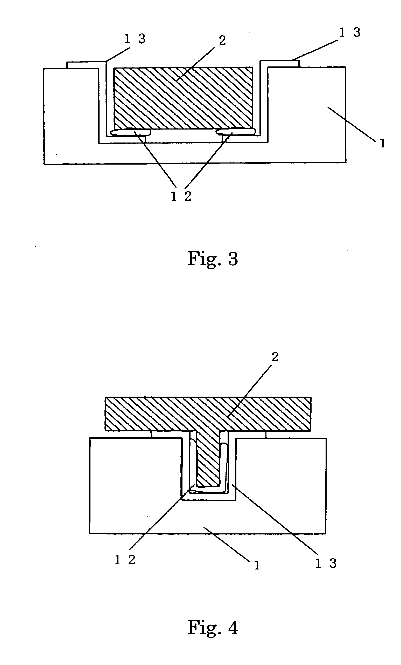
[0050]FIG. 5 is a sectional view of an electronic circuit device having a silicon substrate according to Embodiment 3 of the present invention. The silicon substrate 1 has a front surface and a back surface. The upper side of FIG. 5 corresponds to the front surface, and the lower side thereof corresponds to the back surface. The elements such as a transistor, resistor, and capacitor are formed on the front surface of the silicon substrate 1 by using the silicon planar process.
[0051] A point of difference from the embodiment in FIG. 3 is that the recess of the silicon substrate has two levels. The shape of the recess thus eases the insertion of the passive element 2 from the front surface of the silicon substrate.
[0052] Further, as the shape of the recess, a tapered shape can also be made by conducting taper etching through anisotropic wet etching and then conducting DRIE vertically, as shown in FIG. 6. This structure further eases the insertion of the passive element 2 from the fr...
PUM
 Abstract
Description
Claims
Application Information