Semiconductor device and manufacturing method for the same
- Summary
- Abstract
- Description
- Claims
- Application Information
AI Technical Summary
Benefits of technology
Problems solved by technology
Method used
Image

Examples
embodiment 1
1. EMBODIMENT 1
[0049] Described below is a semiconductor memory pertaining to an embodiment 1 of the present invention.
1-1. Circuit Structure of Semiconductor Memory
[0050] The circuit structure of a semiconductor memory pertaining to the present embodiment is described firstly.
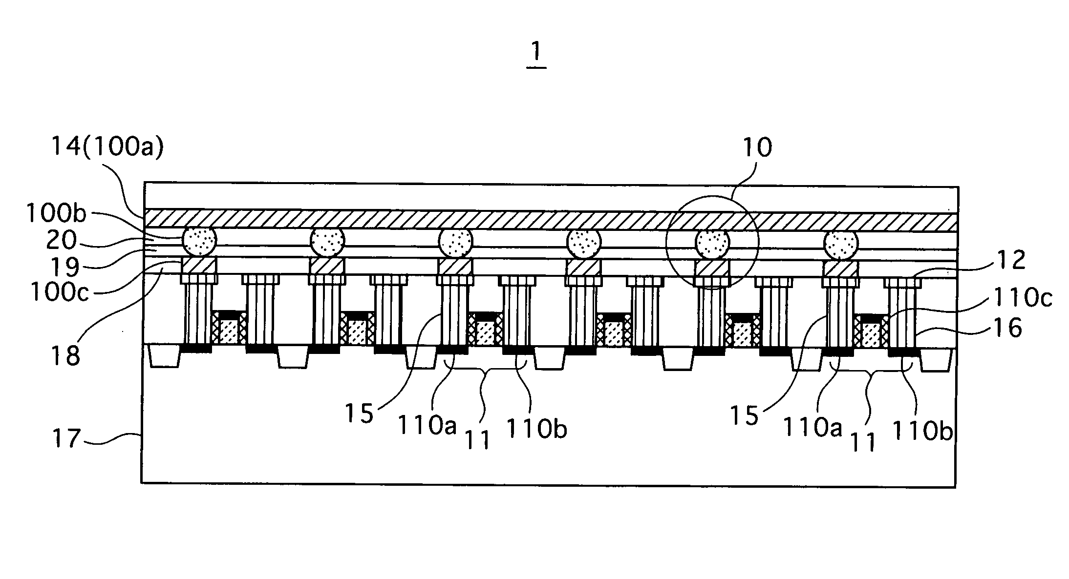
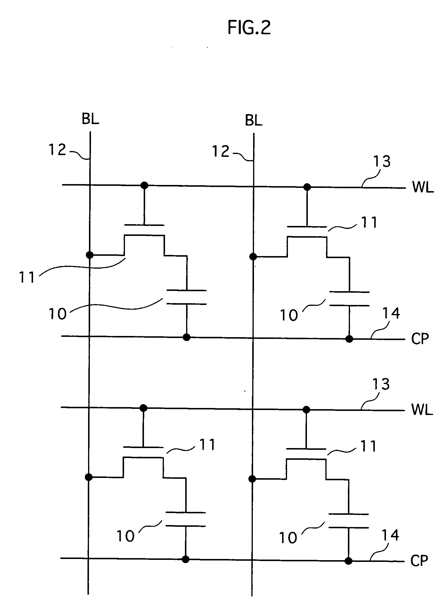
[0051]FIG. 2 is a circuit diagram of a main portion of the circuit structure of a semiconductor memory pertaining to the present embodiment. As shown in FIG. 2, semiconductor memory 1 includes devices 10, transistors 11, bit lines 12, word lines 13, and cell plate lines 14.
[0052] Here, devices 10 include a resistor layer that employs metal-insulator phase transition material, one electrode of the device being connected to a source electrode of a respective transistor 11, while the other electrode is connected to a respective cell plate line 14. A drain electrode of each transistor 11 is connected to a respective bit line 12, and a gate electrode is connected to a respective word line 13.
[0053] According ...
embodiment 2
2. EMBODIMENT 2
[0068] An embodiment 2 of the present invention is described next. While a semiconductor memory pertaining to the present embodiment includes a similar structure to the semiconductor memory pertaining to embodiment 1, a difference lies in the method for selectively placing resistor particles. The present embodiment is thus described only in terms of the manufacturing method for the devices having resistor particles.
[0069]FIGS. 7A to 7E show the processes for selectively placing resistor particles with respect to the semiconductor memory pertaining to the present embodiment. In FIGS. 7A to 7E, the manufacturing method begins from a state in which components corresponding to transistors 11, electrodes 100c and the like in embodiment 1 have already been made.
[0070] Firstly, as shown in FIG. 7A, an electrode 41 is formed on a semiconductor substrate 40, and an insulating film 42 is then formed on electrode 41. A through-hole 42h is formed in insulating film 42, exposing...
embodiment 3
3. EMBODIMENT 3
[0078] Embodiment 3 of the present invention is described next. A feature of a semiconductor memory pertaining to the present embodiment is, in addition to the structure of the semiconductor memories pertaining to embodiments 1 and 2, the three-dimensional placement of memory arrays, thus improving the placement density of memory cells.
[0079]FIG. 8 is a cross-sectional view showing the structure of a semiconductor memory pertaining to the present embodiment. In the present embodiment, as shown in FIG. 8, firstly a semiconductor memory 50 the same as semiconductor memory 1 shown in FIG. 3 is manufactured, and an interlayer insulating film 51a is formed on semiconductor memory 50. After polishing interlayer insulating film 51a to a flat surface, semiconductor thin films 52a are formed on interlayer insulating film 51a, and electrodes 53a are formed on semiconductor thin film 52a. Semiconductor thin film 52a and electrodes 53a are then etched into the shape shown in FIG...
PUM
 Abstract
Description
Claims
Application Information
 - R&D
- Intellectual Property
- Life Sciences
- Materials
- Tech Scout
- Unparalleled Data Quality
- Higher Quality Content
- 60% Fewer Hallucinations
Browse by: Latest US Patents, China's latest patents, Technical Efficacy Thesaurus, Application Domain, Technology Topic, Popular Technical Reports.
© 2025 PatSnap. All rights reserved.Legal|Privacy policy|Modern Slavery Act Transparency Statement|Sitemap|About US| Contact US: help@patsnap.com