CMOS image sensor for processing analog signal at high speed

a high-speed, image sensor technology, applied in the field of cmos image sensors, can solve the problems of reducing the reliability and productivity of the devices, the timing margin of stabilizing a signal value within a settling time is small, and the conventional system cannot achieve high-speed operation

Inactive Publication Date: 2005-10-27
CROSSTEK CAPITAL
View PDF10 Cites 25 Cited by
  • Summary
  • Abstract
  • Description
  • Claims
  • Application Information

AI Technical Summary

Benefits of technology

[0011] It is, therefore, an object of the present invention to provide a CMOS image sensor, in which a high-speed operation can be achieved even though a low-speed system (for example, ASP) is used.

Problems solved by technology

For these reasons, the conventional system cannot achieve high-speed operation.
Also, if a high-speed system is designed, a timing margin for stabilizing a signal value within a settling time is small.
Therefore, the reliability and productivity of the devices are degraded.

Method used


Image

  • CMOS image sensor for processing analog signal at high speed
  • CMOS image sensor for processing analog signal at high speed
  • CMOS image sensor for processing analog signal at high speed

Examples


first embodiment

[0023] First Embodiment

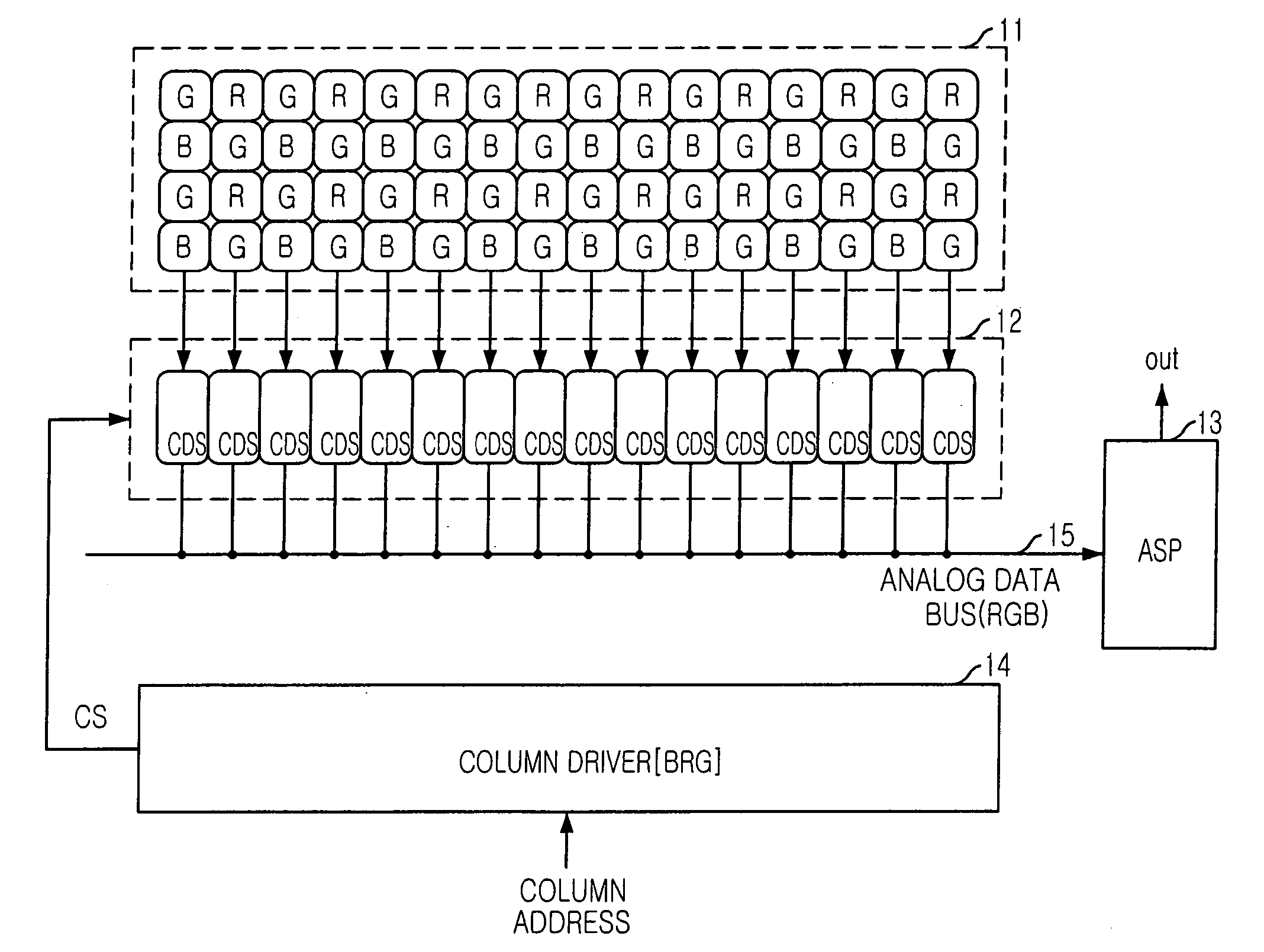
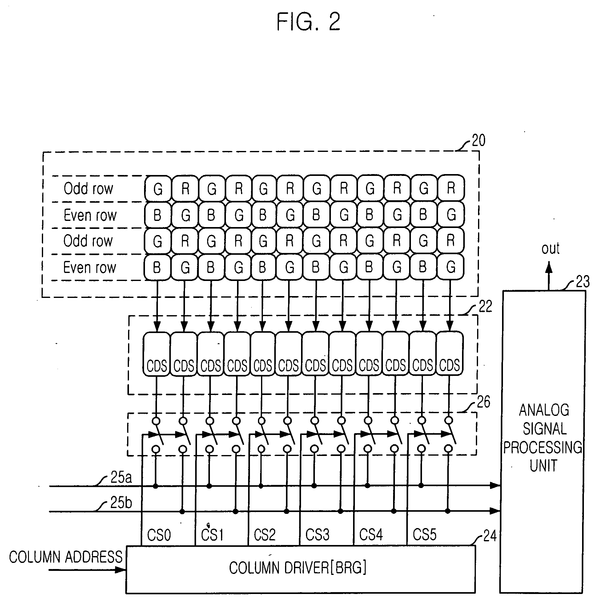
[0024]FIG. 2 is a diagram of a CMOS image sensor in accordance with a first embodiment of the present invention. Image data (analog signals) obtained from pixels are processed through two extended buses 25a and 25b.

[0025] Referring to FIG. 2, the CMOS image sensor includes a pixel array 20 where red (R), green (G) and blue (B) pixels are arranged in an M N matrix form. A CDS part 22 including CDS circuits is provided at a lower side of the pixel array 20. In the CDS part 22, one CDS circuit per column is provided. An analog signal processor (ASP) 23 is provided at a right side of the pixel array 20 to process the analog signals outputted from the CDS part 22. A column driver 24 receives a column address to output column select signals CS0 to CS5, and a selecting part 26 selectively transfers output signals of the CDS circuits to a corresponding analog data bus in response to the column select signals CS0 to CS5.

[0026] The pixel array 20 includes a plurality ...

second embodiment

[0033] Second Embodiment

[0034] A CMOS image sensor in accordance with a second embodiment of the present invention uses one ASP and four analog data buses.

[0035] Referring to FIG. 3, the CMOS image sensor includes a pixel array 31 where red (R), green (G) and blue (B) pixels are arranged in an M N matrix form. A CDS part 32 including CDS circuits is provided at a lower side of the pixel array 31. In the CDS part 32, one CDS circuit per column is provided. An analog signal processor (ASP) 33 is provided at a right side of the pixel array 31 to process the analog signals outputted from the CDS part 32.

[0036] The output signals of the CDS part 32 are transferred through the analog data bus to the ASP 33. Unlike the prior art, the analog data bus is extended into first to fourth analog data buses 35a, 35b, 35c and 35d.

[0037] The output signals of the CDS circuits of the CDS part 32 are loaded on the first to fourth analog data buses 35a, 35b, 35c and 35d by a selecting part 36, which...

third embodiment

[0039] Third Embodiment

[0040]FIG. 4 is a diagram of a CMOS image sensor in accordance with a third embodiment of the present invention. An analog signal processing path for processing analog signals outputted from pixels of the pixel array is divided into two.

[0041] Referring to FIG. 4, the CMOS image sensor includes a pixel array 41 where red (R), green (G) and blue (B) pixels are arranged in an M N matrix form. CDS parts 42 and 46 including CDS circuits are provided at lower and upper sides of the pixel array 41. In the CDS parts 42 and 46, one CDS circuit per column is provided. An analog signal processor (ASP) 43 is provided at a right side of the pixel array 41 to process the analog signals outputted from the CDS part 42, and an ASP 47 is provided to process the analog signals outputted from the CDS part 46.

[0042] The pixel array 41 includes a plurality of even rows and a plurality of odd rows. In the even row, a G pixel is arranged in a first column, and a G pixel and an R p...


PUM


Abstract

A CMOS image sensor is provided. In the CMOS image sensor, a pixel array has a plurality of first color pixels, a plurality of second color pixels and a plurality of third color pixels, which are arranged in matrix form. A CDS (correlated double sampling) part has CDS circuits to receive output signals of the pixels, one CDS circuit per column being provided. A plurality of analog data buses receive divided output signal of the CDS circuits. An ASP (analog signal processor) is connected to the plurality of analog data buses.

Description

FIELD OF THE INVENTION [0001] The present invention relates to a CMOS image sensor; and, more particularly, to a CMOS image sensor for processing an analog signal at high speed and a signal processing method therein. DESCRIPTION OF RELATED ART [0002] An image sensor is an apparatus to convert an optical image into an electrical signal. Such an image sensor is largely classified into a complementary metal oxide semiconductor (CMOS) image sensor and a charge coupled device (CCD). [0003] In the case of the CCD, individual MOS capacitors are disposed very close to one another and charge carriers are stored in and transferred to the capacitors. Meanwhile, in the case of the CMOS image sensor, a pixel array is constructed using a CMOS integrated circuit technology and output data are detected in sequence through a switching operation. Since the CMOS image sensor has an advantage of low power consumption, it is widely used in a personal communication system, such as a hand-held phone. [000...

Claims


Application Information

Patent Timeline
Patent Type & Authority Applications(United States)
IPC IPC(8): H04N5/335H01L27/146H04N5/357H04N5/363H04N5/374H04N5/378H04N9/04H04N9/07
CPCH04N2209/045H04N25/77
Inventor KIM, SONG-YIBAE, CHANG-MINKIM, NAM-RYEOLOH, HACK-SOO
Owner CROSSTEK CAPITAL
Why Eureka
Try Eureka