Operation scheme for spectrum shift in charge trapping non-volatile memory

a non-volatile memory and spectrum shift technology, applied in static storage, digital storage, instruments, etc., can solve the problems of poor charge retention, and large vt distribution of erase state, so as to improve endurance and reliability

Active Publication Date: 2005-10-27
MACRONIX INT CO LTD
View PDF79 Cites 130 Cited by
  • Summary
  • Abstract
  • Description
  • Claims
  • Application Information

AI Technical Summary

Benefits of technology

[0010] A method of operating a memory cell, and an architecture for an integrated circuit including such a memory cell, are provided having improved endurance and reliability. A charge balancing operation for charge trapping-type memory cells is described. This charge balancing operation includes a bias arrangement inducing E-field assisted electron ejection from the gate to the channel and/or direct tunneling of holes for embodiments with thin bottom dielectrics, balanced by E-field assisted electron injection from the gate to the charge trapping structure, including applying a negative gate voltage relative to the substrate (either by applying a −VG or a positive substrate voltage +VSUB, or a combination of −VG and +VSUB), wi

Problems solved by technology

Although the erase speed is fast using this technique, the charge retention is poor due to the charge leakage through ultra-thin bottom oxide.
However, the hot hole injection causes oxide damage, leading to charge loss in the high threshold cell and charge gain in the low threshold cell.
This difference in erase speed results in a large Vt distribution of the era

Method used


Image

  • Operation scheme for spectrum shift in charge trapping non-volatile memory
  • Operation scheme for spectrum shift in charge trapping non-volatile memory
  • Operation scheme for spectrum shift in charge trapping non-volatile memory

Examples


Embodiment Construction

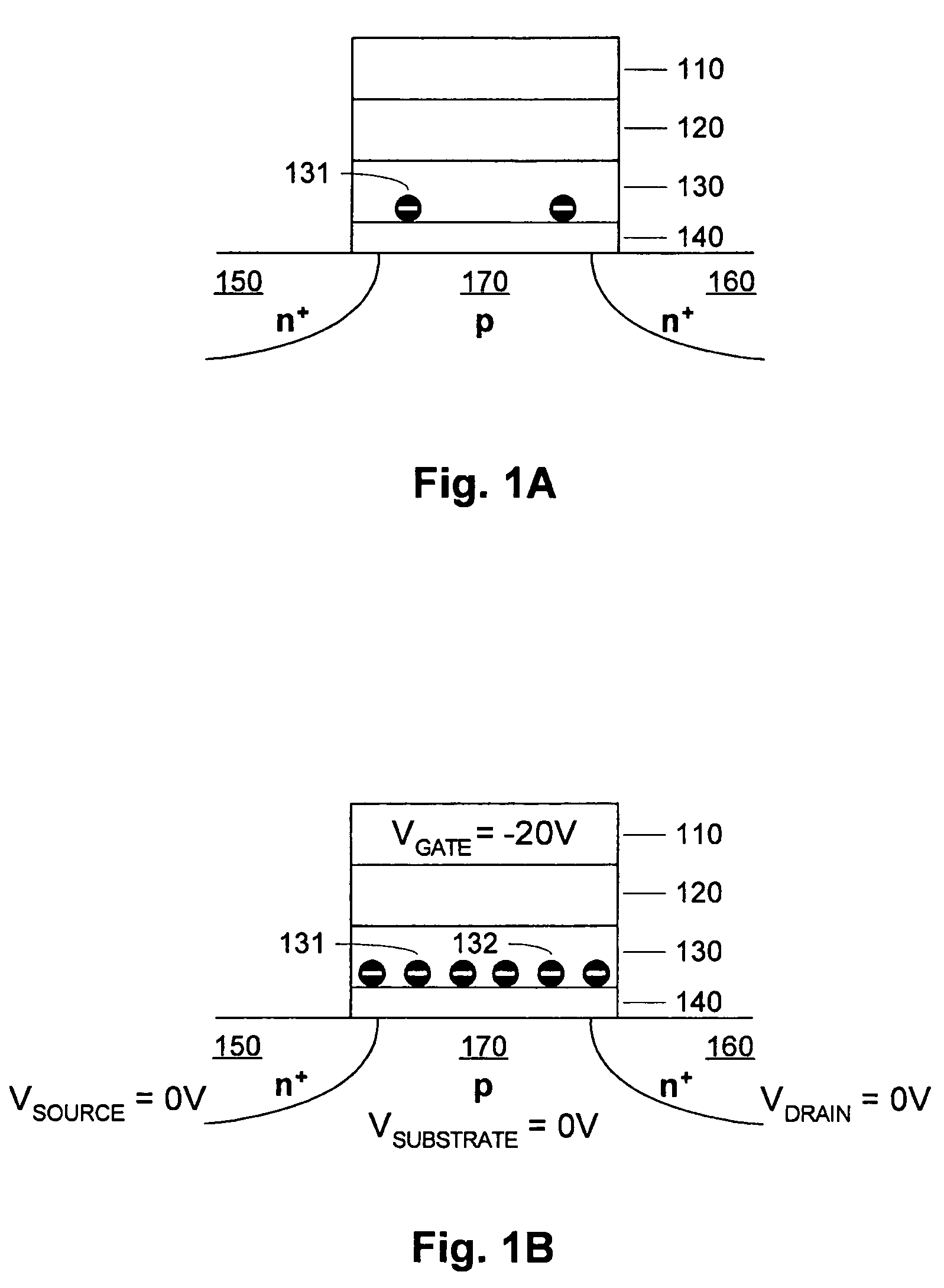
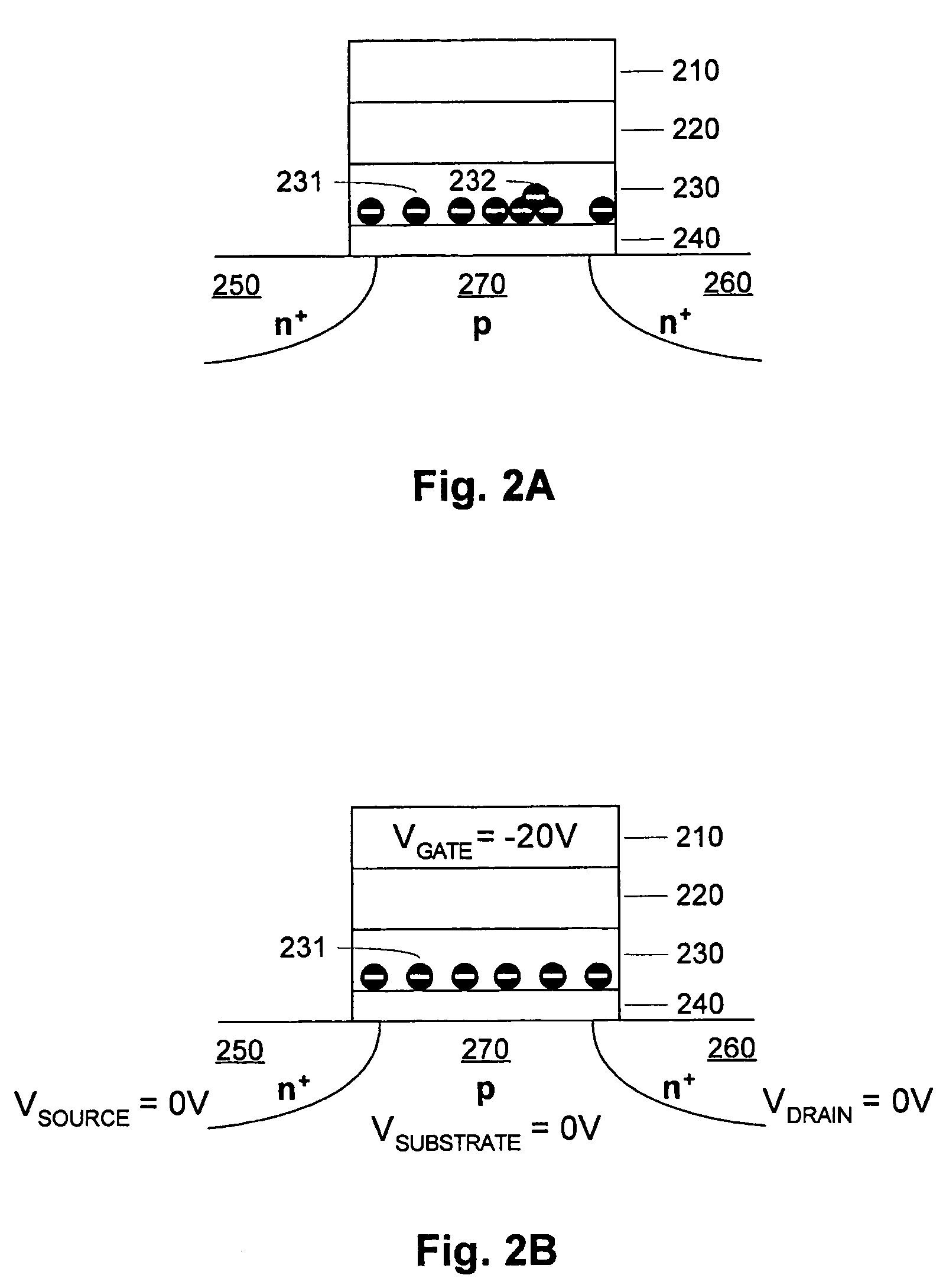
[0069]FIG. 1A is a simplified diagram of a charge trapping memory cell. The substrate includes n+ doped regions 150 and 160, and a p-doped region 170 between the n+ doped regions 150 and 160. The remainder of the memory cell includes a bottom dielectric structure 140 on the substrate, a charge trapping structure 130 on the bottom dielectric structure 140 (bottom oxide), a top dielectric structure 120 (top oxide) on the charge trapping structure 130, and a gate 110 on the oxide structure 120. Representative top dielectrics include silicon dioxide and silicon oxynitride having a thickness of about 5 to 10 nanometers, or other similar high dielectric constant materials including for example Al2O3. Representative bottom dielectrics include silicon dioxide and silicon oxynitride having a thickness of about 3 to 10 nanometers, or other similar high dielectric constant materials. Representative charge trapping structures include silicon nitride having a thickness of about 3 to 9 nanometers...


PUM


Abstract

A memory cell with a charge trapping structure is programmed using refill cycles that include a program pulse followed by a charge balancing pulse that causes ejection of electrons from the charge trapping structure. The refill cycle causes a blue spectrum shift in the charge trap distribution in the charge trapping structure. The algorithm includes program verify operations after the program pulse, and completes when a successful program verify operation occurs after a number of refill cycles.

Description

RELATED APPLICATIONS [0001] The present application claims priority to U.S. Provisional Application No. 60 / 565,377 filed 26 Apr. 2004. The present application also claims priority to U.S. Provisional Application No. 60 / 566,669 filed 30 Apr. 2004.BACKGROUND OF THE INVENTION [0002] 1. Field of the Invention [0003] The present invention relates to electrically programmable and erasable non-volatile memory, and more particularly to charge trapping memory with a bias arrangement, in addition to threshold voltage raising and lowering operations, that modifies the charge in the memory. [0004] 2. Description of Related Art [0005] Electrically programmable and erasable non-volatile memory technologies based on charge storage structures known as EEPROM and flash memory are used in a variety of modern applications. A number of memory cell structures are used for EEPROM and flash memory. As the dimensions of integrated circuits shrink, greater interest is arising for memory cell structures base...

Claims


Application Information

Patent Timeline
IPC IPC(8): G11C11/36G11C16/04G11C16/34
CPCG11C16/0466G11C16/3481G11C16/3436
Inventor LUE, HANG-TINGSHIH, YEN-HAOHSIEH, KUANG YEULEE, MING-HSIUWU, CHAO-IHSU, TZU-HSUAN
Owner MACRONIX INT CO LTD
Why Eureka
Try Eureka