Optical element, optical head, optical information recording/reproduction device, computer, video recording device, video reproduction device, server, and car navigation system
Inactive Publication Date: 2005-10-27
PANASONIC CORP
6 Cites 30 Cited by
AI-Extracted Technical Summary
Problems solved by technology
A problem that occurs at this time is that there is an increase in aberration caused by an inclination of the disk in relation to the light axis (what is known as “tilt”).
When the NA is made large, the aberration caused by tilt increases.
However, in the optical head of the first conventional example, when light is irradiated onto optical disks that have widely different substrate thicknesses, such as a substrate thickness of 1.2 mm and a substrate thickness of 0.1 mm, there is the problem that the distance between the disk and the objective lens changes significantly, the movable range of the actuator increases, and the head becomes large.
Moreover, there is the problem that in order to detect the l...
Benefits of technology
[0036] It is an object of the present invention to solve the foregoing conventional problems, and to provide optical elements, optical heads, optical information recording and reproduction apparatuses, computers, image re...
Abstract
The present invention provides a first light source (21) that emits light of a first wavelength, that at least either records onto or reproduces information from an information recording medium (30), a light source (22) that emits light of a second wavelength that records onto or reproduces information from an information recording medium (33), a light source (23) that emits light of a third wavelength that records onto or reproduces information from an information recording medium (23), focusing means, an optical element (28) that passes light of the first wavelength and diffracts light of the second and third wavelengths, wherein the optical element (28) is an optical element in which grooves are formed in a substrate, wherein the expression:
380 nm≦(n−1)×d≦420 nm
is satisfied, where n is a refractive index of the substrate at a wavelength of 400 nm, and d (nm) is a depth per step of the grooves, and wherein the grooves are formed in two steps of depth d and depth 2d.
Application Domain
Record information storageOptical beam guiding means +2
Technology Topic
Equipment computersNanometre +9
Image
Examples
- Experimental program(15)
Example
First Embodiment
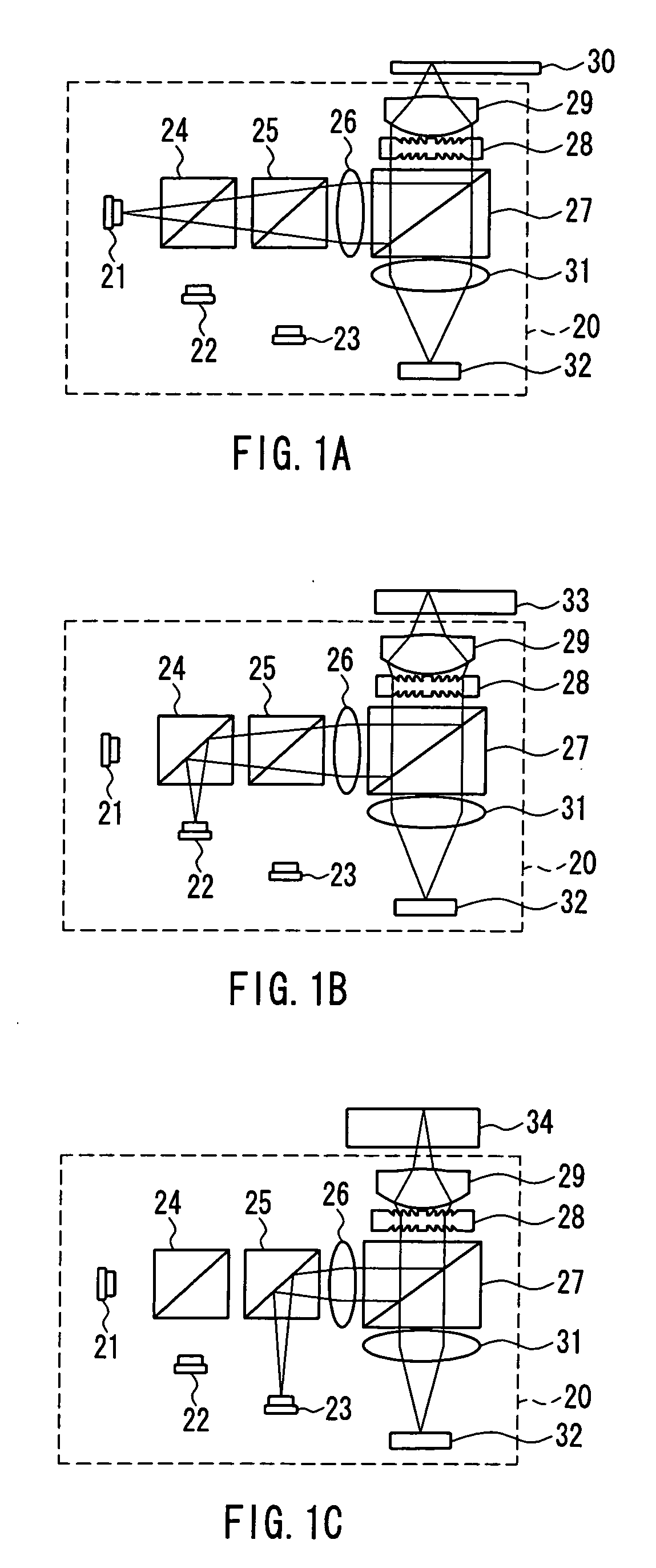
[0484]FIG. 1 shows a structural view of an optical head 20 according to a first embodiment of the present invention. The optical head 20 is capable of at least either recording to or reproducing from (referred to below as “recording and reproduction”) an optical disk. FIG. 1A shows the recording and reproduction state of a high density optical disk whose substrate thickness is thin, FIG. 1B shows the recording and reproduction state of a DVD, and FIG. 1C shows the recording and reproduction state of a CD.
[0485] The optical head 20 is provided with three types of light source; a blue semiconductor laser 21 (light source of a first wavelength) of a wavelength of approximately 400 nm (380 nm to 420 nm), a red semiconductor laser 22 (light source of a second wavelength) of a wavelength of 630 nm to 680 nm, and an infrared semiconductor laser 23 (light source of a third wavelength) of a wavelength of 780 nm to 820 nm.
[0486] When recording and reproducing a high density optical disk 30 (FIG. 1A), light of a wavelength λ1 emitted from the blue semiconductor laser 21 passes through wavelength selecting prisms 24 and 25, and is converted to collimated light by a collimator lens 26. The light that was made parallel is reflected by a beam splitter 27, passes through a dichroic hologram (optical element) 28, is converted to convergent light by an objective lens (focusing means) 29 and is irradiated onto the high density optical disk (a first information recording medium) 30.
[0487] The numerical aperture (NA) of the objective lens 29 is 0.85, and the substrate thickness of the high density optical disk is assumed to be 0.1 mm. The objective lens 29 is designed such that the aberration is at a minimum, that is to say, such that the standard deviation of the wavefront aberration is at a minimum when the blue light of wavelength λ1 is irradiated onto the disk of substrate thickness 0.1 mm. Furthermore, the dichroic hologram 28 is designed so as to allow the light of wavelength λ1 to pass through it without being affected.
[0488] The light that was reflected by the high density optical disk 30, diffracted and modulated, passes again through the objective lens 29 and the dichroic hologram 28, passes through the beam splitter 27, is converted to convergent light by a detecting lens 31, and is incident on a photodetector (a photodetecting means) 32. The photodetector 32 contains a plurality of photodetecting regions, and outputs a signal in response to the amount of light that is received.
[0489] When recording and reproducing a DVD 33 (a second information recording medium) (FIG. 1B), light of a wavelength λ2 emitted from the red semiconductor laser 22 is reflected by the wavelength selecting prism 24, passes through the wavelength selecting prism 25, and is converted to collimated light by the collimator lens 26. The light that was converted to collimated light is reflected by the beam splitter 27, is diffracted and wavefront converted by the dichroic hologram (optical element) 28, converted to converging light by the objective lens 29, and is irradiated onto the DVD 33.
[0490] The numerical aperture (NA) of the light emitted from the objective lens 29 is limited to 0.6. The substrate thickness of the DVD 33 is 0.6 mm. The dichroic hologram 28 is designed such that when the red light of wavelength λ2 irradiates the disk of the substrate thickness 0.6 mm after passing through the objective lens 29, the standard deviation of the wavefront aberration is not more than 70 mλ.
[0491] The light that was reflected by the DVD 33, diffracted and modulated, passes again through the objective lens 29 and the dichroic hologram 28, passes through the beam splitter 27, is converted to converging light by the detecting lens 31, and is incident on the photodetector 32. The photodetector 32 contains a plurality of photodetecting regions, and outputs a signal in response to the amount of light that is received.
[0492] When recording and reproducing a CD 34 (third information recording medium) (FIG. 1C), light of a wavelength λ3 emitted from the infrared semiconductor laser 23 is reflected by the wavelength selecting prism 25, and is converted to collimated light by the collimator lens 26. The light that was converted to collimated light is reflected by the beam splitter 27, is diffracted and wavefront converted by the dichroic hologram (optical element) 28, is converted to converging light by the objective lens 29, and is irradiated onto the CD 34.
[0493] The numerical aperture (NA) of the light emitted from the objective lens 29 is limited to 0.4. The substrate thickness of the CD 34 is 1.2 mm. The dichroic hologram 28 is designed such that when the infrared light of wavelength λ3 irradiates the disk of the substrate thickness 1.2 mm after passing through the objective lens 29, the standard deviation of the wavefront aberration is not more than 70 mλ.
[0494] The light that was reflected by the CD 34, diffracted and modulated, passes again through the objective lens 29 and the dichroic hologram 28, passes through the beam splitter 27, is converted to converging light by the detecting lens 31 and is incident on the photodetector 32. The photodetector 32 contains a plurality of photodetecting regions, and outputs a signal in response to the amount of light that is received.
[0495]FIG. 2A shows an upper surface pattern of the dichroic hologram, and FIG. 2B shows a rear surface pattern. The light that approaches the disk enters from the rear surface (first optical element) 40 and exits from an upper surface (second optical element) 41. Light of wavelength λ3, which is in a range of 780 nm to 820 nm, is diffracted in a region 42 of the rear surface 40, and a pattern is formed so as to provide a wavefront that is optimal to the CD 34 (such that the standard deviation of the wavefront aberration is not more than 70 mλ when focusing on the CD 34).
[0496] The light of wavelength λ3 passes through the upper surface 41 without being affected. Furthermore, the light of wavelength λ2, which is in a range of 630 to 680 nm, is diffracted by the pattern in the region 42 of the rear surface 40, after which it is also diffracted by the pattern that is formed in a region 43 on the upper surface 41.
[0497] The pattern within the region 43 is formed such that the light of wavelength λ2 that was diffracted by both upper and rear surfaces has an optimal wavelength for the DVD 33 (such that when focusing on DVD 33, the standard deviation of the wavefront aberration is not more than 70 mλ). Because the principal object of the upper surface 41 and the rear surface 40 is to apply power to the diffracted light and to correct spherical aberration, the pattern is concentric ring-shaped. Light in the vicinity of wavelength λ1=400 nm passes through both upper and rear surfaces without being affected.
[0498]FIG. 3 shows an enlarged cross-section of the rear surface 40 of the dichroic hologram 28. The rear surface 40 of the dichroic hologram is engraved with grooves that have four types of depth (d to 4d). These grooves are configured in a repeating pattern of a group of grooves that are lined up as a single group in the order of 2d, 4d, d, 3d and no-groove portion.
[0499] Here, depth d is: [0500] d=λ1/(n1−1)
where n1 is the refractive index of a medium at the wavelength λ1, which is selected from within the range 380 to 420 nm. The phase shift in the light of wavelength λ1 that occurs due to the light path difference between the indented groove portion and the no-groove portion is an integer multiple of 2π by satisfying this relationship. That is to say, the light path length (n1−1)×d is equivalent to the wavelength λ1. Due to this, light of the blue semiconductor laser of wavelength λ1 passes through the dichroic hologram 28 unaffected (it is not diffracted).
[0501] If the wavelength is fixed, the light path length expressed by (n1−1)×d has a unique value, and the effect that the light that is within the wavelength range 380 to 420 nm passes substantially through the dichroic hologram 28 can be obtained if the light path length is within a predetermined range.
[0502] More specifically, it is preferable that the expression:
380 nm≦(n1−1)×d≦420 nm
is satisfied when the standard wavelength, from the range 380 to 420 nm of wavelengths of λ1, is 400 nm, and n is the refractive index of the substrate at a wavelength of 400 nm.
[0503] On the other hand, light of wavelength λ2 of the red semiconductor laser has a modulated wavefront as shown in FIG. 4A. Because the light of wavelength λ2 that records and reproduces DVDs is in the range 630 nm to 680 nm, d is a depth that is equivalent to approximately 0.6 times the length of wavelength λ2.
[0504] Consequently, 2d is 1.2λ, 3d is 1.8λ and 4d corresponds to 2.4λ. If each value is an integer multiple of λ then the phase shift of the light does not occur, so that with regards to the phase of the light, integer multiples of λ can be ignored. Thus, considering only the fractional parts smaller than the decimal point, d is 0.6λ, 2d is 0.2λ (1.2λ−1λ), 3d is 0.8λ (1.8λ−1λ), and 4d corresponds to 0.4λ (2.4λ−2λ).
[0505] Consequently the grooves arranged in the order of 2d, 4d, d and 3d form wavefronts that have stepwise phase changes of 0.2λ, 0.4λ, 0.6λand 0.8λ with respect to the light of wavelength λ2 as shown in FIG. 4B. That is to say that with respect to the light of wavelength λ2, the grooves shown in FIG. 3 can be thought of as grooves that deepen in a stepwise manner in the direction from the 2d side to the 3d side, as shown in FIG. 4B.
[0506] When grooves such as those shown in FIG. 3 are formed on the incident face side (a boundary at which the light propagates from a medium of low refractive index (such as air) to a one of a high refractive index (such as glass)) of an optical element, the intensity of light that is diffracted in a direction 1 (the direction from the groove depth 3d side toward the groove depth 2d side) of FIG. 3 is stronger than light that is diffracted in a direction 2 (the direction from the groove depth 2d side toward the groove depth 3d side).
[0507] Here, FIG. 5 shows the relationship between the groove depth of a single step that is standardized with respect to the wavelength λ, and an efficiency R, which is the efficiency of incident light that is converted to first order diffracted light by a dichroic hologram such as that whose cross-section is shown in FIG. 3. When the depth that corresponds to a single step is 0.6 times λ, the diffraction efficiency is at its maximum, and it is possible to obtain a diffraction efficiency greater than 0.8.
[0508] Furthermore, a wavefront of the light of wavelength λ3 of the infrared semiconductor laser is modulated as shown in FIG. 6A. Because λ3 is in a range of 780 nm to 820 nm for the purpose of recording and reproducing CDs, d is a depth equivalent to approximately 0.5 times the length of wavelength λ3.
[0509] Consequently, 2d is 1.0λ, 3d is 1.5λ and 4d is equivalent to 2.0λ. As described previously, as the phase of the light, the integer multiple portions of λ can be ignored, so if only the portions smaller than the decimal point are considered, then d is 0.5λ, 2d is 0 (1.0λ−1λ), 3d is 0.5λ (1.5λ−1λ) and 4d is equivalent to 0 (2.0λ−2λ). Consequently, the grooves arranged in the order of 2d, 4d, d, 3d form wavefronts that have a two step phase of 0, 0, 0.5λ, 0.5λ, whose duty ratio is 3:2 with respect to light of wavelength λ3 as shown in FIG. 6B. In this case, according to FIG. 5, a diffraction efficiency of about 0.3 can be obtained when the depth corresponding to a single step is 0.5 times λ.
[0510]FIG. 7 shows an enlarged cross-sectional view of the upper surface 41 of the dichroic hologram 28. The upper surface of the dichroic hologram 28 is engraved with grooves of three different depths (d to 3d). These grooves are configured as a single group in a repeating pattern of a group of grooves that are lined up in an order of d, 2d, 3d, and no-groove portion. Depth d is: [0511] d=2×λ1/(n1−1)
when n1 is the refractive index of a medium at a wavelength λ1, which is selected from the range 380 to 420 nm. By satisfying this relationship, the phase shift in the light of wavelength λ1 that occurs due to the light path difference between the indented portion, which is the groove, and the no-groove portion is an integer multiple of 2π. Due to this, light of the blue semiconductor laser of wavelength λ1 passes through unaffected by the dichroic hologram 28 (it is not diffracted).
[0512] In this case, the light path length, which is (n1−1)×d, is equivalent to two times the wavelength λ1. As described previously, if the light path length is within a predetermined range then it is possible to achieve the effect that light of a wavelength, which is in a range of 380 to 420 nm, can substantially pass through the dichroic hologram 28.
[0513] More specifically, it is preferable that the expression:
760 nm≦(n1−1)×d≦840 nm
is satisfied when the standard wavelength, from the range 380 to 420 nm of wavelengths of λ1, is 400 nm, and n is the refractive index of the substrate at a wavelength of 400 nm.
[0514] On the other hand, the light of wavelength λ2 of the red semiconductor laser has a modulated wavefront as shown in FIG. 8A. Because the light of wavelength λ2 that records and reproduces DVDs is in the range λ2=630 nm to 680 nm, d is a depth that corresponds to approximately 1.2 times the length of wavelength λ2.
[0515] Consequently, 2d is 2.4λ and 3d is 3.6λ. As previously described, integer multiple portions of λ can be ignored for phases of the light, so if only the fractional parts smaller than the decimal point are considered, d is 0.2λ(1.2λ−λ), 2d is 0.4λ (2.4λ−2λ) and 3d is 0.6λ (3.6λ−3λ).
[0516] Consequently the grooves arranged in the order of d, 2d, and 3d form wavefronts that have stepwise phase changes of 0.2λ, 0.4λ, and 0.6λ with respect to light of wavelength λ2 as shown in FIG. 8B. That is to say that, with respect to the light of wavelength λ2, the grooves shown in FIG. 7 can be considered as grooves that deepen in a stepwise manner in the direction from the d side to the 3d side, as shown in FIG. 8B.
[0517] When grooves such as those shown in FIG. 7 are formed on the incident face side of an optical element (a boundary at which the light propagates from one of a high refractive index (such as glass) to a medium of low refractive index (such as air)), the intensity of light that is diffracted in a direction 1 (the direction from the groove depth 3d side toward the groove depth d side) of FIG. 7 is stronger than light that is diffracted in a direction 2 (the direction from the groove depth d side toward the groove depth 3d side).
[0518]FIG. 9A shows the relationship between the groove depth of a single step that is standardized with respect to the wavelength λ, and an efficiency R, which is the efficiency of incident light that is converted to first order diffracted light by a dichroic hologram 28 such as is shown in FIG. 7. When the depth corresponding to a single step is 1.2 times λ, a diffraction efficiency higher than 0.65 can be obtained.
[0519] Furthermore, the light of wavelength λ3 of the infrared semiconductor laser has a wavefront that is modulated as shown in FIG. 8C. Because λ3 is in a range of 780 nm to 820 nm for the purpose of recording and reproducing CDs, d is a depth equivalent to approximately 1.0 times the length of wavelength λ3. Consequently, 2d is 2.0λ and 3d is equivalent to 3.0λ. As described previously, as the phase of the light, the integer multiple portions of λ can be ignored, so if only the portions smaller than the decimal point are considered then all are equivalent to 0 as shown in FIG. 8d. Consequently, the light of wavelength λ3 is unaffected by the dichroic hologram 28 (it is not diffracted), and substantially passes through it.
[0520] Here, FIG. 9B shows the relationship between the groove depth of a single step that is standardized with respect to the wavelength λ, and an efficiency R, which is the efficiency of incident light that is converted to zero order diffracted light by a dichroic hologram such as is shown in FIG. 7. When the depth corresponding to a single step is 1.0 times λ, it is possible to obtain a transmittance of approximately 0.9.
[0521] In this way the light of wavelength λ1 at the rear surface (first optical element) 40 passes though the dichroic hologram 28 substantially without being affected, while the light of wavelength λ2 and wavelength λ3 are diffracted. Furthermore, at the upper surface (second optical element) 41, the light of wavelength λ1 and λ3 pass through and the light of wavelength λ2 is diffracted.
[0522] Due to this, information can be recorded and reproduced reliably because light sources that have appropriate wavelengths for each of the three types of optical disks (information recording media) are used and light of low aberration can be focused on the information surface with excellent efficiency. Furthermore, the same effect also can be obtained when there are two types of optical disk.
[0523] It should be noted that the dichroic hologram 28 used here has the first optical element and the second optical element formed on the upper surface 41 and the rear surface 40 as a single piece. However it is also possible to arrange a dichroic hologram such that the first optical element and the second optical element are formed on separate elements. In that case, their centers can be matched up to the optical axis by adjusting the position of both optical elements.
[0524] Furthermore, it is preferable that the dichroic hologram 28 is fabricated from glass. If it is fabricated from resin, then it is preferable to use amorphous polyolefin based resins whose absorbtance is not more than 5%, and whose absorptance is preferably not more than 3%. This is due to the fact that light of a wavelength of not more than 420 nm has a strong chemical action, so there is a possibility that the resin may be damaged if an optical element of high absorptance is irradiated over a long period. It is relatively difficult to damage amorphous polyolefin based resins, even by irradiating with light of a wavelength less than 420 nm.
[0525] Moreover, it is also possible to fabricate one of the optical elements on the surface of the objective lens. In this case, it is possible to increase the positional accuracy of the optical axis of the objective lens.
[0526] Furthermore, the diffraction efficiency shown here is a value that is calculated when the widths of adjacent grooves of different depths are substantially equivalent.
[0527] Furthermore, even if the grooves are lined up in a sequence that is completely opposite to the examples given here, the same effect can be obtained apart from a change in the direction in which the light is efficiently diffracted.
[0528] Furthermore, it goes without saying that even if the start point of the way the grooves are lined up, and the way the grooves are described is changed, if the grooves are actually lined up in the same sequence, then the same effect can be obtained.
[0529] Moreover, the wavelengths λ1 and λ2 satisfy the relationship
1.5≦λ2/λ1≦1.8,
and the wavelengths λ1 and λ3 satisfy the relationship
1.8≦λ3/λ1≦2.2.
[0530] Furthermore, as shown in FIG. 10, the light of wavelength λ2, which is diffracted by the dichroic hologram 28 is designed such that the diffraction efficiency of the light of wavelength λ2 that is diffracted from collimated light to diverging light (direction 1) by the dichroic hologram 28, is greater than the diffraction efficiency on the side in which it is diffracted to converging light (direction 2). More specifically, grooves such as are shown in FIG. 3 are arranged in a concentric ring shape on the incident face such that the direction 1 approaches the circumference, and the direction 2 approaches the center, and moreover, on the exit face side, grooves such as are shown in FIG. 7 are arranged in a concentric ring-shape such that the direction 1 approaches the circumference, and the direction 2 approaches the center. In this way, because the diffraction efficiency in the direction 1 is higher than the diffraction efficiency in the direction 2, the diffracted light is substantially converted to diverging light, and the dichroic hologram 28 acts as a concave lens.
[0531] Thus, a focal length f of the focusing optical system, which is matched to the objective lens, lengthens and even DVDs, which at 0.6 have a thicker substrate than a substrate thickness of 0.1, can be operated at a relatively large working distance.
[0532] It should be noted that there is no particular discussion here of methods for limiting the aperture of the light of wavelength λ2 or the light of wavelength λ3, however there is the method of vapor depositing a wavelength selecting filter onto the dichroic hologram 28 or the objective lens 29, or the method of providing a separate glass filter. Furthermore, it is also possible to control the aperture by providing an opening across the light path that is passed only by light of a single wavelength (in the region between the light source and the wavelength selecting prism).
[0533]FIG. 11 shows an entire structural example of an optical disk drive 50 as an optical information recording and reproduction apparatus. An optical disk 51 is fixed by sandwiching between a turntable 52 and a damper 53, and is rotated by a motor (rotating system) 54, which is a moving means. An optical head 20 is mounted on a traverse (conveying system) 55, which is a moving means, and the point that is irradiated by light is capable of moving from the inner circumference of the optical disk 51 to the outer circumference. The control circuits 56 perform focus control, tracking control, traverse control and rotational control of the motor and the like based on signals received from the optical head 20.
[0534]FIG. 12 shows the working distance when recording and reproducing each disk. The height of the side at which light is incident on the optical disk is determined by the position of the turntable 52. On the other hand, the relative height of fixing elements 60 on the actuator of the optical head 20 with respect to the turntable 52 is determined uniquely by the structure and the positional relationship of the traverse 55 and the motor 54. Furthermore, the position of a movable element 61 of the actuator that moves the objective lens 29 in the focus direction is determined by the position of the recording surface of the optical disk, and by back focus on the disk side of the objective lens 29, which is the focusing means. Back focus means the length between the tip of the focusing means to the point of convergence of the light rays. The tip of the focusing means more specifically that, of the intersections between the objective lens 29 and the optical axis, it is the intersection that is on the optical disk side.
[0535] The working distance WD is
WD=BF−t/n
when the refractive index at the wavelength λ is n, the substrate thickness of the disk is t and the back focus is BF. For example, on a disk in which the substrate thickness is thick, and t/n is large, the working distance WD becomes small such that if the focusing means not designed such that the back focus BF can change in response to that change, then the working distance WD will vary greatly when there is a change in substrate thickness.
[0536]FIG. 12 shows the working distance WD at a working distance WD1 (FIG. 12A), a working distance WD2 (FIG. 12B) and a working distance WD3 (FIG. 12C), depending on the type of optical disk, that is, depending on changes in the substrate thickness.
[0537] A configuration according to a conventional example is shown in FIG. 13, showing the case in which a working distance changes greatly depending on the type of optical disk. When there is a large change in working distance due to the type of the optical disk, there is a large change in the relative distance between the fixing elements 60 of the actuator and the movable element 61.
[0538] Because a working distance WDa in FIG. 13A is small, the movable element 61 is relatively higher than the upper side (disk side) of the fixing elements 60. However as in FIG. 13B, when the working distance WDb is large, the moving element 61 is relatively lower than the lower side (side furthest from the disk) of the fixing elements 60. Because regular optical disks droop on their inner and outer circumferential sides and have shake of disc in focusing direction when rotating, to a certain extent the fixing elements 60 cover the vertical movement range of the movable element 61. However, when there is a difference in working distance, there is a problem in that to absorb that difference, the size of the actuator increases, and the overall size of the optical head. increases. Furthermore, when the movable range is large, the movable element 61 tilts depending on the position of the movable element 61, and there is the problem that the optical system is susceptible to generating aberrations.
[0539] The moveable range of the moveable element 61 also depends on the structure of the actuator, however it is preferable that it is less than the lateral direction width of the moveable element 61. This is because, if the lateral width is large, even if a height difference develops between left and right, then the tilting angle is small. However, if the lateral width is small, even with a minimal left and right height difference, the tilting angle becomes large.
[0540] Consequently, the difference in working distance caused by disk type, that is to say, the movable range of the movable element 61 is preferably smaller than the lateral width of the movable element 61. In the example of FIG. 12, it is preferable that the maximum and minimum differences between WD1, WD2 and WD3, being the difference in working distance caused by disk type, are smaller than the lateral width of the movable element 61.
[0541] In the case of the ultra high density optical disk, when NA=0.85, and the focal length f of the focusing means is 2.0 mm, the beam diameter is φ3.4 mm. Because the minimum value of the width of the movable element 61 is this beam width, in this case there is a need to set the difference between the maximum value and minimum value of the working distance to 3.4 mm at most.
[0542] It should be noted that when considering the actual size of the actuator, the movement range of the actuator is at best 1 mm, so that it is preferable that the difference between the maximum working distance and minimum working distance is not more than half that at 0.5 mm. Moreover, in order not to substantially affect the size of the actuator, it is preferable that the difference between the maximum value and the minimum value of the working distance is not more than 0.2 mm. Of course, the most preferable state is the one in which the working distance is equivalent when recording onto and reproducing information from differing types of information recording media, and in which the difference between the maximum value and the minimum value is 0.
[0543] In the present embodiment, since the back focus BF can be set optimally using the dichroic hologram 28 according to the disk that is recorded or reproduced, the WD can be substantially fixed during recording and reproduction of each disk.
[0544] More specifically, in the example given previously, light from the blue semiconductor laser (wavelength λ1) is not diffracted by the dichroic hologram 28, and the diffraction efficiency of the light from the red semiconductor laser (wavelength λ2) is set to differ from the diffraction efficiency of the light from the infrared semiconductor laser (wavelength λ3). Thus, light of the blue semiconductor laser passes as is through the dichroic hologram 28, the degree of divergence of the light of the red semiconductor laser differs from the degree of divergence of the light of the infrared semiconductor laser, and it is possible to change the back focus depending on the light from each laser. That is to say, it is possible to design the dichroic hologram 28 so as to control the back focus depending on the type of disk, and it is possible to substantially fix the WD without consideration to the type of disk.
[0545] If the WD can be substantially fixed in this way, then the size of the entire optical head can be reduced, and because the movable range of the movable element 61 can be reduced, it is possible to suppress the generation of aberrations caused by tilt of the movable element 61.
[0546]FIG. 14 shows an example that unifies the signal output from the optical head of the present embodiment. An optical head 70 has the same optical structural elements as the optical head 20. It differs in the provision of a P/S (parallel/serial) converting circuit 71 (parallel/serial converter) that converts the output signal from the photodetector 32 that is received as a parallel signal into a serial signal. A P/S converting circuit 71 receives signals through a plurality of signal lines from the photodetector 32, time divides and lines them up serially, and outputs them as an output signal through a single signal line.
[0547] As a method for this, there is the method of sequentially switching an analog switch in an internal portion of the P/S converting circuit based on the clock, which is a timing signal, and outputting the serial signal as an output signal. Furthermore, a method is also possible in which the signal that is obtained in parallel is subjected to analog/digital conversion (A/D conversion), stored in memory and then transmitted as digital data in a serial sequence. FIG. 15 shows an example of the signal in such a case. Synchronised with the clock as the timing signal, digital signals such as an RF signal, and FE+ signal, an FE− signal, a TE+ signal and a TE− signal and the like are transmitted.
[0548] Thus, the number of signal lines between the optical head and the control circuits and the like of the optical disk drive can be reduced. In optical heads that record and reproduce CDs and DVDs as well as high density optical disks, approximately three times the usual amount of signal lines are necessary just to drive the semiconductor lasers, which are the light source. FIG. 14A shows an example in which the photodetector (photodetecting means) is shared, and as shown in FIG. 14B, also conceivable is a case in which the photodetector (photodetecting means) is not shared, and which has the photodetector (photodetecting means) 72 and a photodetector (photodetecting means) 73, and a case which contains three photodetectors. In these cases, there is a further increase in signal lines, the width of the flexible cable that connects the optical head and the drive is enlarged, and there is the problem of a loss of flexibility (the ease of bending) of the flexible cable. Furthermore, if the flexible cable is changed to a multilayer flexible circuit, then although the width of the flexible cable can be reduced, there is the problem of an increase in cost.
[0549] If the optical head is an optical head 75 that is provided with a P/S converting circuit 74 for receiving signals in parallel from the photodetector 72 and the photodetector 73, and outputting them as serial signals such as is shown in FIG. 14B, then the number of signal lines can be greatly reduced.
[0550] In the example of the optical head 75 in FIG. 14B, the signal from the P/S converting circuit 74 is converted to an optical signal by an LED (electrical/optical converter) 76 and is output to an optic fiber 77. In this case, it is possible to transmit a higher frequency signal than an electric signal yet with lower noise, and there is the advantage that these signals can be transmitted with sufficient accuracy and period of time even if there is an increase in the number of signals to be converted.
[0551] It should be noted that the example in which the P/S converting circuit is utilized is not limited to optical heads in which light sources of three wavelengths are used, and the same effect can be obtained with optical heads containing light sources of one wavelength or two wavelengths. In these cases as well, if a plurality of signal lines are needed for tracking signals or focus signals, then the optical head can be consolidated into a single unit. Furthermore, if A/D conversion is performed within the optical head, then because paths that introduce noise can be shortened, this is also effective in raising the SN ratio of the signal.
Example
Second Embodiment
[0552] An example of an optical head applied interchangeably to high density optical disks and DVDs is described as a second embodiment. FIG. 16 is a structural example of an optical head 80. As shown in FIG. 16A, a light of wavelength λ1 emitted from a blue semiconductor laser (a light source of a first wavelength) 21 passes through the wavelength selecting prism 24, and is converted to collimated light by the collimator lens 26. The light that was converted to collimated light is reflected by the beam splitter 27, passes through the dichroic hologram (optical element) 81, is focused by the objective lens (focusing means) 29 and is irradiated onto the high density optical disk (first information recording medium) 30.
[0553] The numerical aperture (NA) of the objective lens is 0.85, and the substrate thickness of the high density optical disk 30 is assumed to be 0.1 mm. The objective lens 29 is designed such that spherical aberration is at a minimum when the blue light of wavelength λ1 is radiated onto a disk whose substrate thickness is 0.1 mm.
[0554] Furthermore, the dichroic hologram 81 is designed so as to pass the light of wavelength λ1 without affecting it. The light that was reflected by the high density optical disk 30, diffracted and modified, again passes through the objective lens 29 and the dichroic hologram 81, passes through the beam splitter 27, is focused by the detecting lens and is incident on a photodetector (photodetecting means) 82. The photodetector 82 contains a plurality of photodetecting regions, and outputs a signal in response to the amount of light that is received.
[0555] As shown in FIG. 16B, when recording and reproducing the DVD 33 (second information recording medium), the light of wavelength λ2 is emitted from the red semiconductor laser 22, is reflected by the wavelength selecting prism 24 and is converted to collimated light by the collimator lens 26. The light that was converted to collimated light is reflected by the beam splitter 27, is diffracted by the dichroic hologram 81 and wavefront converted, is focused by the objective lens 29 and is irradiated onto the DVD 33.
[0556] Here, the numerical aperture (NA) of the light that is emitted from the objective lens is limited to 0.6. The substrate thickness of the DVD 33 is 0.6 mm. The dichroic hologram 81 is designed such that when the red light of wavelength λ2 that has passed through the objective lens 29 is irradiated on to the disk of substrate thickness of 0.6 mm, the standard deviation of wavefront aberration is not more than 70 mλ.
[0557] The light that was reflected at the DVD 33, diffracted and modulated, again passes through the objective lens 29 and the dichroic hologram 81, passes through the beam splitter 27, is focused by the detecting lens 31, and is incident on the photodetector 82. The photodetector 82 contains a plurality of photodetecting regions, and outputs a signal in response to the amount of light that is received.
[0558]FIG. 17 shows a pattern on the upper surface (the disk side) and the rear side (the side that is furthest from the disk) of the dichroic hologram 81. The light that approaches the disk passes through from the rear surface to the upper surface. No particular pattern is formed on the rear surface shown in FIG. 17B. On the upper surface that is shown in FIG. 17A, the light in the range of wavelength λ2=630 to 680 nm is diffracted by a pattern within a region 83.
[0559] The pattern within the region 83 is formed such that the light of wavelength λ2 that was diffracted at the upper surface has a wavefront that is optimal for the DVD 33. Since the principal object is to apply power to the diffracted light and to correct spherical aberration, the pattern is concentric ring-shaped. Light in the vicinity of wavelength λ1=400 nm passes through both upper and lower surfaces without being affected.
[0560] The cross-sectional form of the hologram that is formed on the upper surface of the dichroic hologram 81 is the same as the cross-sectional form of that which is formed on the rear surface 40 of the dichroic hologram 28 of the first embodiment. Accordingly, because high diffraction efficiencies can be obtained for the light of wavelength λ2 that is in the range 630 to 680 nm, satisfactory light utilization efficiency can be achieved.
[0561] Consequently, since it is possible to use light sources whose respective wavelengths are appropriate to the types of optical disks (information recording media), namely high density optical disks 30 and DVDs 33, and to focus light with less aberrations onto the information surfaces at high efficiencies, information can be recorded and reproduced reliably.
[0562] As in the present embodiment, by setting the surface of the dichroic hologram 81 on which the pattern is provided to be the face closest to the objective lens, it is possible to prevent the minimum pitch of the dichroic hologram 81 from becoming too small, thus facilitating fabrication of the dichroic hologram 81.
[0563] Furthermore, because recording and reproduction of CDs is omitted from the present embodiment, not only is a light source for CDs unnecessary, but the shape of the dichroic hologram 81 is simplified, and since the variety of signals that the photodetector 82 detects is reduced, the photodetector is simpler than that of the first embodiment.
[0564] Furthermore, FIG. 18 shows an optical head 84 that uses a dichroic hologram 85 in place of the dichroic hologram 81. FIG. 18A is a structural overview of the high density optical disk 30 during recording and reproduction, and FIG. 18B is a structural overview of the DVD 33 during recording and reproduction. FIG. 19 shows a pattern on an upper surface (disk side) and rear surface (side furthest from the disk) of the dichroic hologram 85. The upper surface of the dichroic hologram 85 that is shown in FIG. 19A has the same pattern that is formed on the upper surface of the dichroic hologram 81 shown in FIG. 17. A pattern, which is a hologram for correcting chromatic aberration in light of wavelength λ1, is formed in a region 87 on the rear surface of the dichroic hologram 85 shown in FIG. 19B.
[0565] Holograms for correcting chromatic aberrations are explained in detail in the Patent Document 3 (JP 2001-60336A). In this specification, the cross-section of the optical element is saw tooth-shaped, and a method is described whereby second order diffracted light is used for correcting light of a first wavelength λ1, and first order diffracted light is used for correcting light of a second wavelength λ2. Aberration that occurs at the objective lens caused by wavelength offset of the light of wavelength λ1 is cancelled out by changes in the diffracting angle of the diffraction grating to correct chromatic aberration. Accordingly chromatic aberration can be corrected without the addition of new parts.
[0566] Furthermore, an example of an optical head is described in the present embodiment. However, as in the structure in FIG. 11 of the first embodiment, by providing moving means such as a conveying system 55 or a rotating system 54, and a control circuit 56, the optical head can be used as an optical information recording and reproduction apparatus (optical disk drive).
Example
Third Embodiment
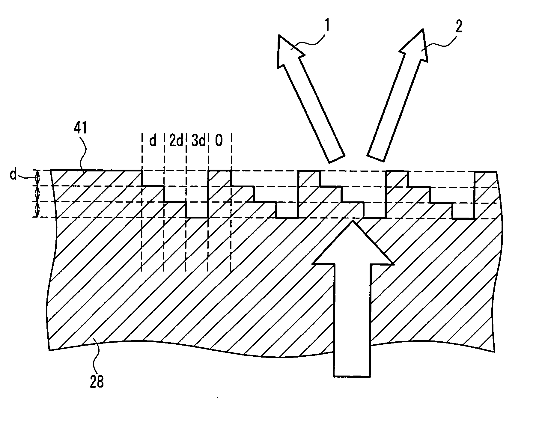
[0567] A third embodiment shows an example of a head that records and reproduces information onto three types of optical disks using three types of light sources using an optical element that has a dichroic hologram on one face and a phase shift step on an opposite face. Furthermore, a dichroic hologram that has two types of groove depths is described.
[0568]FIG. 20 is a structural overview of an optical head 90 according to the present embodiment. Parts that are the same as in the first and second embodiment are given the same symbols, and the description thereof is hereby omitted. The present embodiment differs from the first and second embodiments in the use of a dichroic hologram (optical element) 91, which has a phase shift step on its rear surface.
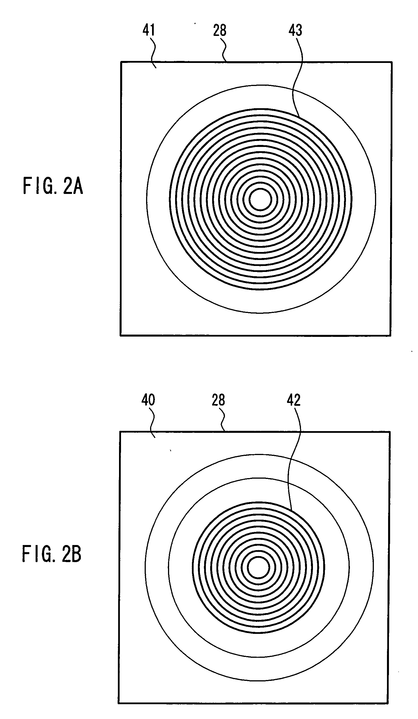
[0569] A front view of the dichroic hologram 91 is shown in FIG. 21, while FIG. 21A shows an upper surface (disk side), FIG. 21B shows a rear surface (side furthest from the disk), and FIG. 21C is a cross-sectional view of FIG. 21B. As shown in FIG. 21A, grooves are formed as a dichroic hologram in a circle-shaped region 93 (first region) in the vicinity of the center of an upper surface 92, and in a ring-shaped region 94 (second region) that wraps around the region 93. No grooves are formed in a region 95 (third region) that is on the outer side of the region 94.
[0570] On the other hand, as shown in FIG. 21B, a phase shift step (phase correcting means) 97 is formed on a rear surface 96. The light of wavelength λ1=380 nm to 420 nm passes as is through the dichroic hologram on the upper surface, but the light of wavelength λ2=630 nm to 680 nm and the light of wavelength λ3=780 nm to 820 nm is diffracted. The light of wavelength λ1 passes through the region 93 and the region 94 and one part of the region 95.
[0571] The light of wavelength λ3 that reproduces the CD 34 passes through the rear surface 96, after which it irradiates only onto the region 93 of the upper surface 92. The pattern of the region 93 is designed such that when the light of wavelength λ3 that was diffracted is irradiated onto the CD 12 of t=1.2 mm, the standard deviation of the wavefront aberration is not more than 70 mλ.
[0572] The phase shift step 97 of the rear surface 96 shown in FIG. 21B is a step that does not affect the light of wavelength λ1 and the light of wavelength λ3. The light of wavelength λ2 is phase modulated by the phase shift step 97 of the rear surface 96, and is irradiated onto the circle-shaped region 93 (first region) and the ring-shaped region 94 (second region) of the upper surface 92.
[0573] The shape of the pattern in the ring-shaped region 94 and the phase shift step 97 (phase correcting means) is designed such that the standard deviation of the wavefront aberration is not more than 70 mλ when the light that was diffracted at the circle-shaped region 93 and the ring-shaped region 94 is irradiated onto the DVD 33 of t=0.6.
[0574]FIG. 22 shows an enlarged cross-sectional view of the dichroic hologram 91. The surface of the dichroic hologram 91 is engraved with grooves that have two types of depths (d and 2d). Those grooves form sets of grooves lined up in the order d, 2d, no groove, and are formed as a repetition of those sets. Where a refractive index of a medium at wavelength λ1 that is within the range of 380 nm to 420 nm is n1, the depth d is expressed by:
d=λ1/(n1−1).
Accordingly, the light of wavelength λ1 from the blue light semiconductor laser passes through without any effect.
[0575] Furthermore, as described in the first embodiment, if the light path length is within a predetermined range, then the effect that light within the wavelength range 380 nm to 420 nm substantially passes through the dichroic hologram can be obtained. Thus, it is preferable that the expression:
380 nm≦(n−1)×d≦420 nm
is satisfied, where n is the refractive index of the substrate at a wavelength of 400.
[0576] On the other hand, the wavefront of the light of wavelength λ2 of the red semiconductor laser is modulated as shown in FIG. 23A. Since the wavelength λ2 is in the range 630 nm to 680 nm for recording and reproduction of the DVD 33, d has a depth that corresponds to approximately 0.6 times the length of the wavelength λ2. Consequently, 2d corresponds to 1.2λ. Since the integer multiples of λ can be ignored in the phases of light, with consideration given only to the portion on the right of the decimal point, d corresponds to 0.6λ and 2d corresponds to 0.2λ. Consequently, grooves that are lined up in the order d, 2d form wavefronts having phases that change stepwise as 0.6λ and 0.2λ, as shown in FIG. 23B.
[0577]FIG. 24 shows the relationship between a groove depth of a single step that is normalized by the wavelength λ, and the efficiency R of converting incident light to first order diffracted light at the dichroic hologram, such as is shown in FIG. 22. From FIG. 24, a diffraction efficiency in the order of 0.6 can be obtained when the depth of one step is 0.6 times λ.
[0578] Furthermore, the wavefront of the light of wavelength λ3 of the infrared semiconductor laser is modulated as shown in FIG. 25A. Since the wavelength λ3 is in the range 780 nm to 820 nm for CD recording and reproduction, d has a depth that corresponds to approximately 0.5 times the length of wavelength λ3. Consequently, 2d corresponds to 1.0λ. Since the integer portions of λ can be ignored in the phases of light, with consideration given only to the part to the right of the decimal point, d corresponds to 0.5λ and 2d corresponds to 0.
[0579] Consequently, grooves that are lined up in the order d, 2d, form wavefronts having two step phases are 0.5λ and 0 as shown in FIG. 25B, whose duty ratio is 1:2. Due to this, a diffraction ratio in the order of 0.3 can be obtained when the depth of one step is 0.5 times λ, as shown in FIG. 24.
[0580] If the dichroic hologram 91 as shown in FIG. 21 is used, then the hologram pattern is only fabricated on one face, and since the rear surface is constituted by a phase shift step that has low light-intensity-loss, light utilization efficiency can be raised.
[0581] Thus, since it is possible to use light sources having wavelengths that are appropriate to the three types of optical disks (information recording media) to focus low aberration light onto the information surface at high efficiency, information can be recorded and reproduced reliably.
[0582] It should be noted that here, the dichroic hologram and the phase shift step are formed on the upper surface and rear surface of a single optical element. However it is also possible to arrange a member in which these are formed on separate optical elements. In this case, by tuning the position of both optical elements, it is possible to adjust their centers to the optical axis.
[0583] Furthermore, the diffraction efficiency shown here is a value calculated when the width of adjacent grooves of various depths is substantially equivalent.
[0584] Moreover, the relationship between the wavelengths λ1 and λ2 satisfies:
1.5≦λ2/λ1≦1.8,
and the relationship between the wavelengths λ1 and λ3 satisfies:
1.8≦λ3/λ1≦2.2.
[0585] The conventional example disclosed in Patent Document 1 (JP H9-306018A), is illustrated by an example that has three types of groove depths, which allows one wavelength to pass through and diffracts another wavelength. However, there is no mention of the fact that when the wavelengths of λ1 and λ2 have the relationship:
1.5≦λ2/λ1≦1.8,
a dichroic hologram that has two types of groove depths, or a dichroic hologram that has four types of groove depths in which these groove depths are lined up in the order 2d, 4d, d, 3d, no groove, can increase the diffraction efficiency of light of wavelength λ2. This is subject matter that is first disclosed by the present invention. Furthermore, the fact that an appropriate diffraction ratio of light of the wavelength λ3 that has the relationship:
1.8≦λ3/λ1≦2.2.
can be obtained with the aforementioned dichroic hologram is another original disclose of the present invention.
[0586] It should be noted that it is also possible that the hologram that is grouped with the phase shift step is of the shape that has four types of groove depths that are shown in the first embodiment. Similarly, it is also possible to use a dichroic hologram of a form having two types of groove depths, as shown in the third embodiment, applied to the dichroic hologram of the first embodiment.
[0587] It should be noted that for simplicity, the light sources here are separate, and the photodetector is shared, however a single light source such as a monolithic semiconductor laser also can be used as the lightsource, and the photodetectors also can be separate. Even with this configuration, the same effect can be demonstrated.
[0588] Furthermore, a disk whose substrate thickness t=0.1 and numerical aperture is 0.8 has been assumed as the example of the high density optical disk. However it is not limited to this.
[0589] Also, although the present embodiment has been described using the example of an optical head, by providing a moving means such as the traverse system 55 or the rotating system 54, and the control circuit 56, it can be used as the optical information recording and reproduction apparatus (optical disk drive), as shown in FIG. 11 of the first embodiment.
PUM


Description & Claims & Application Information
We can also present the details of the Description, Claims and Application information to help users get a comprehensive understanding of the technical details of the patent, such as background art, summary of invention, brief description of drawings, description of embodiments, and other original content. On the other hand, users can also determine the specific scope of protection of the technology through the list of claims; as well as understand the changes in the life cycle of the technology with the presentation of the patent timeline. Login to view more.