Material for substrate mounting optical circuit-electric circuit mixedly and substrate mounting optical circuit-electric circuit mixedly

a technology of optical circuit and substrate, which is applied in the direction of dielectric characteristics, insulating substrate metal adhesion improvement, instruments, etc., can solve the problems of low accuracy of wiring when forming electrical circuits, difficult to manufacture high-quality optical circuit-electrical circuits, and large number of steps. , to achieve the effect of simple method and high quality

Active Publication Date: 2005-10-27
PANASONIC INTELLECTUAL PROPERTY MANAGEMENT CO LTD
View PDF7 Cites 49 Cited by
  • Summary
  • Abstract
  • Description
  • Claims
  • Application Information

AI Technical Summary

Benefits of technology

[0007] Considering the above described problems, the present invention has an object of providing a material for an optical circuit-electrical circuit mixedly mounting substrate which allows the production of the optical circuit-electrical circuit

Problems solved by technology

The methods mentioned above have such problems that a number of steps is large which are required for stacking by forming the optical circuit and the electrical circuit successively.
The accuracy of wiring is low when form

Method used


Image

  • Material for substrate mounting optical circuit-electric circuit mixedly and substrate mounting optical circuit-electric circuit mixedly
  • Material for substrate mounting optical circuit-electric circuit mixedly and substrate mounting optical circuit-electric circuit mixedly
  • Material for substrate mounting optical circuit-electric circuit mixedly and substrate mounting optical circuit-electric circuit mixedly

Examples


example 1

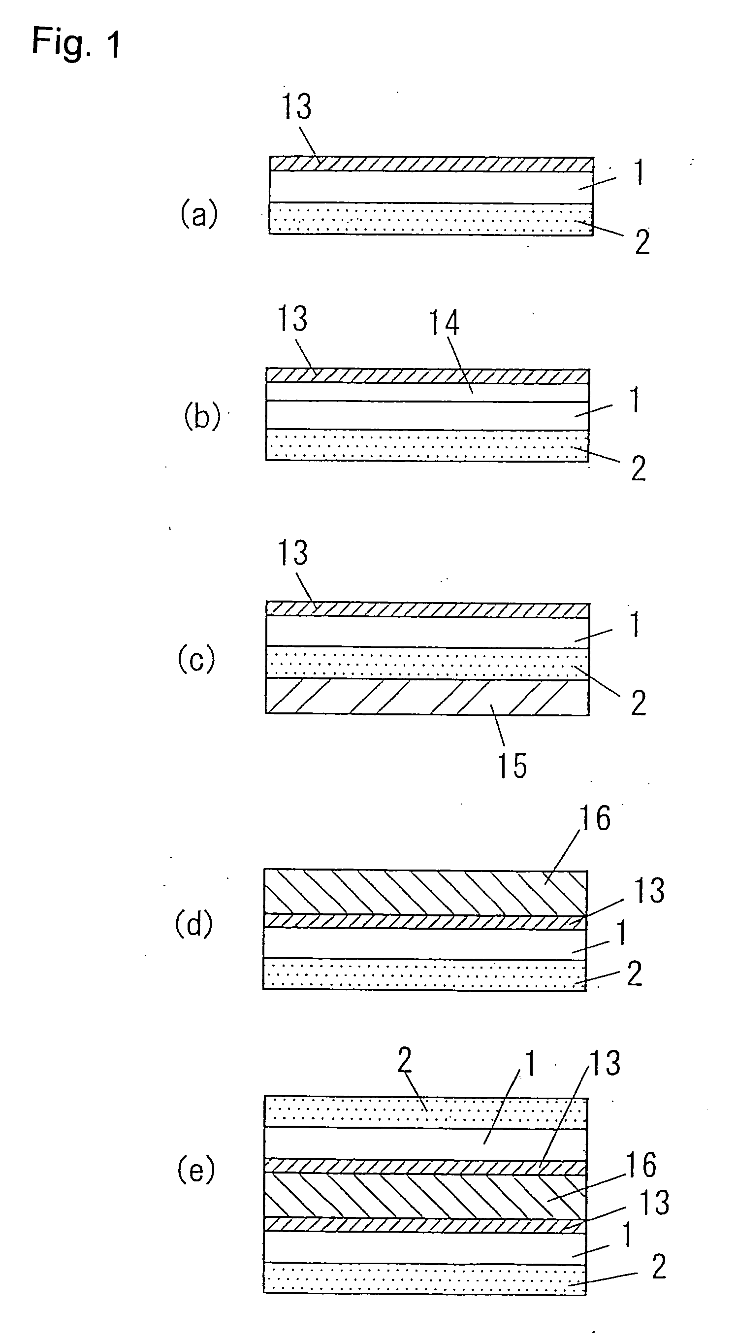
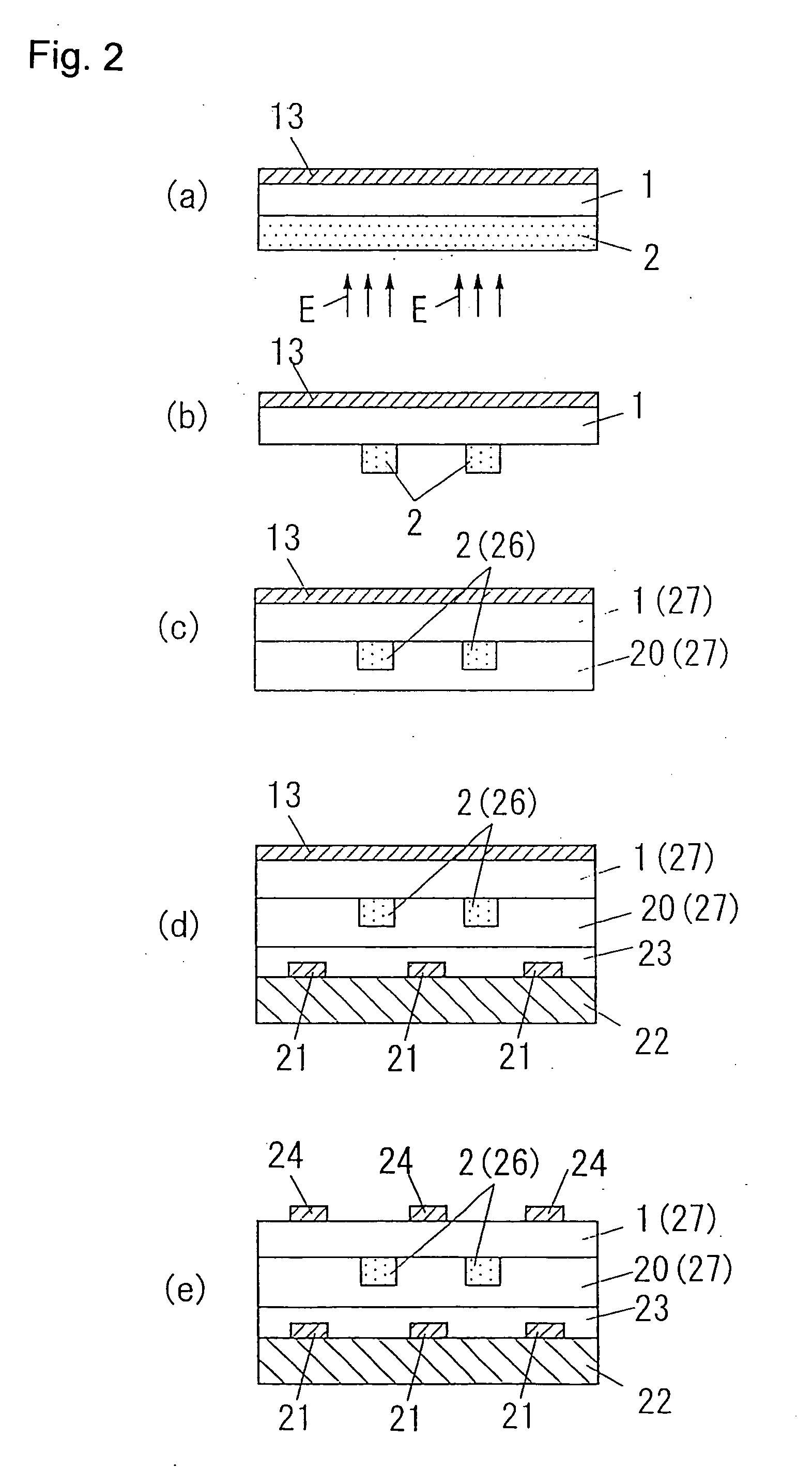
[0394] Using a copper foil having a thickness of 35 μm (“MPGT” manufactured by Furukawa Electric Co., Ltd.) as a metal layer 13, a light permeable resin A was applied to the metal layer 13 by roll transferring process to have a thickness of 50 μm, which was then cured by irradiating with light generated by a high-pressure mercury vapor lamp having an output power of 2.5 J / cm2 to form a light permeable resin layer 1. Then, a varnish which contains a photosensitive resin A was applied to a thickness of 80 μm and heated to dry so as to form an optical circuit forming layer 2 having a thickness of 40±5 μm, thereby to obtain the material for the optical circuit-electrical circuit mixedly mounting substrate as shown in FIG. 1(a).

[0395] As the light permeable resin A, “Optodyne UV-3100” manufactured by Daikin Industries, Ltd. was used, which is a UV-curing epoxy resin that has a refractive index of 1.49 after being cured.

[0396] AS the vanish which contains the photosensitive resin A, a v...

example 2

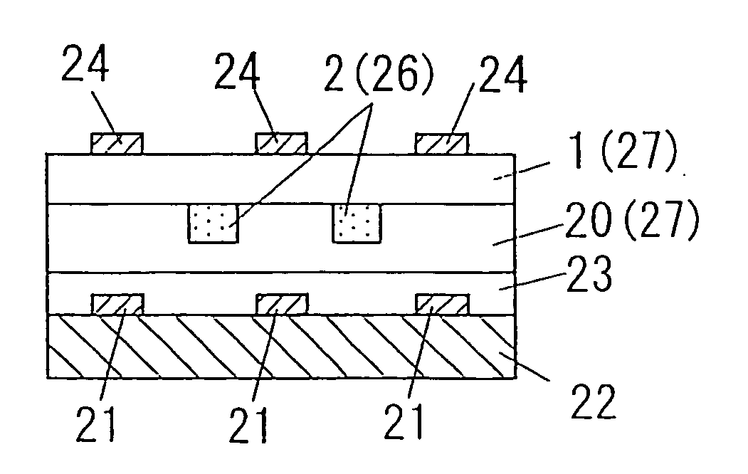
[0400] In Example 1, after forming the optical circuit forming layer 2, a cover film 15 made of a transparent PET having a thickness of 25 μm was laminated on the surface of the optical circuit forming layer 2 by pressing with a roller, to obtain the material for the optical circuit-electrical circuit mixedly mounting substrate as shown in FIG. 1(c), which showed good workability of handling because the optical circuit forming layer 2 was not exposed.

[0401] The material for the optical circuit-electrical circuit mixedly mounting substrate was processed similarly to Example 1, except that after exposing to irradiation through the cover film 15, developing was carried out while removing the cover film 15, so as to obtain the optical circuit-electrical circuit mixedly mounting substrate. Testing the obtained optical circuit-electrical circuit mixedly mounting substrate similarly to Example 1 showed that the optical circuit was functioning. Measurement of peel-off strength of the coppe...

example 3

[0402] Using a copper foil as the metal layer 13 similarly to Example 1, the adhesive varnish A was applied on the metal layer 13 to a thickness of 40 μm and dried at 150° C., and thereby the adhesive layer 14 was formed. By forming the light permeable resin layer 1 and the optical circuit forming layer 2 on the adhesive layer 14 similarly to Example 1, the material for the optical circuit-electrical circuit mixedly mounting substrate shown in FIG. 1(b) was obtained.

[0403] The material for the optical circuit-electrical circuit mixedly mounting substrate was processed similarly to Example 1, thereby to obtain the optical circuit-electrical circuit mixedly mounting substrate. Testing the optical circuit-electrical circuit mixedly mounting substrate similarly to Example 1 showed that the optical circuit was functioning. Measurement of peel-off strength of the copper foil constituting the metal layer 13 showed a strength of 9.8 N / cm (1.0 kg / cm), proving that bonding strength of the me...


PUM

PropertyMeasurementUnit
Timeaaaaaaaaaa
Solubility (mass)aaaaaaaaaa
Permeabilityaaaaaaaaaa

Abstract

A material for an optical circuit-electrical circuit mixedly mounting substrate comprises a light permeable resin layer, and an optical circuit forming layer that is made of a light permeable resin of which refractive index increases (or decreases) when irradiated with an activating energy beam and is disposed adjacent to the light permeable resin layer, wherein a refractive index of a portion of the optical circuit forming layer is higher (or lower) than that of the light permeable resin layer when the material for the optical circuit-electrical circuit mixedly mounting substrate is irradiated with an activating energy beam so that said portion is irradiated.

Description

TECHNICAL FIELD [0001] The present invention relates to a material which can be used as a raw material for manufacturing a substrate including an optical circuit (a circuit that transmits light) and an electrical circuit (or electrical wiring) together, that is a substrate which mounts an optical circuit and an electrical circuit mixedly (or together) (hereinafter which substrate is also referred to as an “optical circuit-electrical circuit mixedly mounting substrate”), and a method for manufacturing the optical circuit-electrical circuit mixedly mounting substrate. According to the present invention, the optical circuit and the electrical circuit may respectively be a part thereof, and in this respect the optical circuit and the electrical circuit may be an optical line or an optical waveguide and an electrical wiring, respectively. The optical circuit-electrical circuit mixedly mounting substrate is also referred to as an “electrical-optical circuit board.”BACKGROUND ART [0002] Re...

Claims


Application Information

Patent Timeline
IPC IPC(8): G02B6/12G02B6/122G02B6/13G02B6/138G02B6/42G02B6/43H05K1/02H05K3/38H05K3/46
CPCB32B15/08G02B6/12004G02B6/13G02B6/138G02B6/43Y10T428/24942H05K3/386H05K3/4652H05K2201/0108H05K2201/0195H05K1/0274
Inventor NAKASHIBA, TOORUKOTERA, KOUHEIMATSUSHIMA, TOMOAKIMATSUSHITA, YUKIONAKANISHI, HIDEOHASHIMOTO, SHINJINEMOTO, TOMOAKIYAGYU, HIROYUKIKASAI, YUUKI
Owner PANASONIC INTELLECTUAL PROPERTY MANAGEMENT CO LTD
Why Eureka
Try Eureka