Pixel clock generation circuit

a technology of pixel clock and generation circuit, which is applied in the direction of generating/distributing signals, pulse automatic control, printing, etc., can solve the problems of electrostatic latent images, image quality degradation, and image quality degradation, and achieve the effect of simple structur

Inactive Publication Date: 2005-11-03
RICOH KK
View PDF5 Cites 57 Cited by
  • Summary
  • Abstract
  • Description
  • Claims
  • Application Information

AI Technical Summary

Benefits of technology

[0010] Accordingly, it is a general object of the present invention to provide a pixel clock generation circuit that can c...

Problems solved by technology

This change in scanning speed may cause the fluctuation of images, and results in the degradation of image quality.
If the chromatic aberration of the multi-beam optical system is not adjusted, the difference in frequencies may cause the positions of formed electrostatic latent images.
This means that the range on the surface of the photosensitive unit 4004 in which each light spot scans may differ from each other, and r...

Method used


Image

  • Pixel clock generation circuit
  • Pixel clock generation circuit
  • Pixel clock generation circuit

Examples


Embodiment Construction

[0055] The preferred embodiments of the present invention are described in detail below with reference to the drawings.

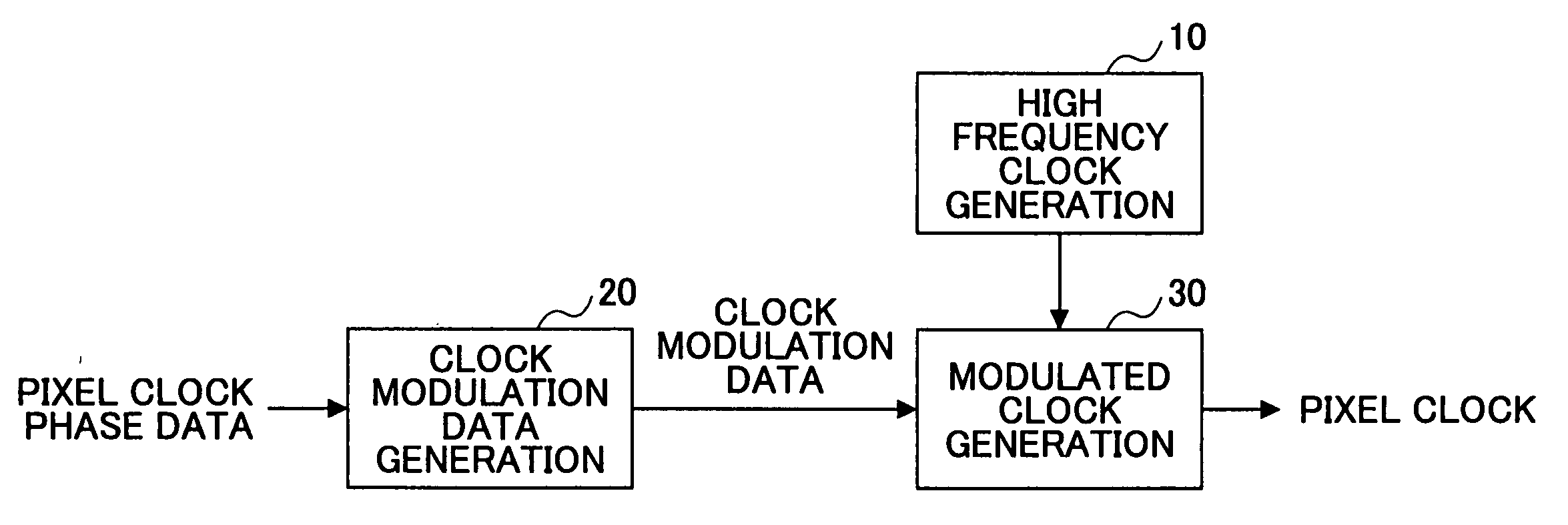
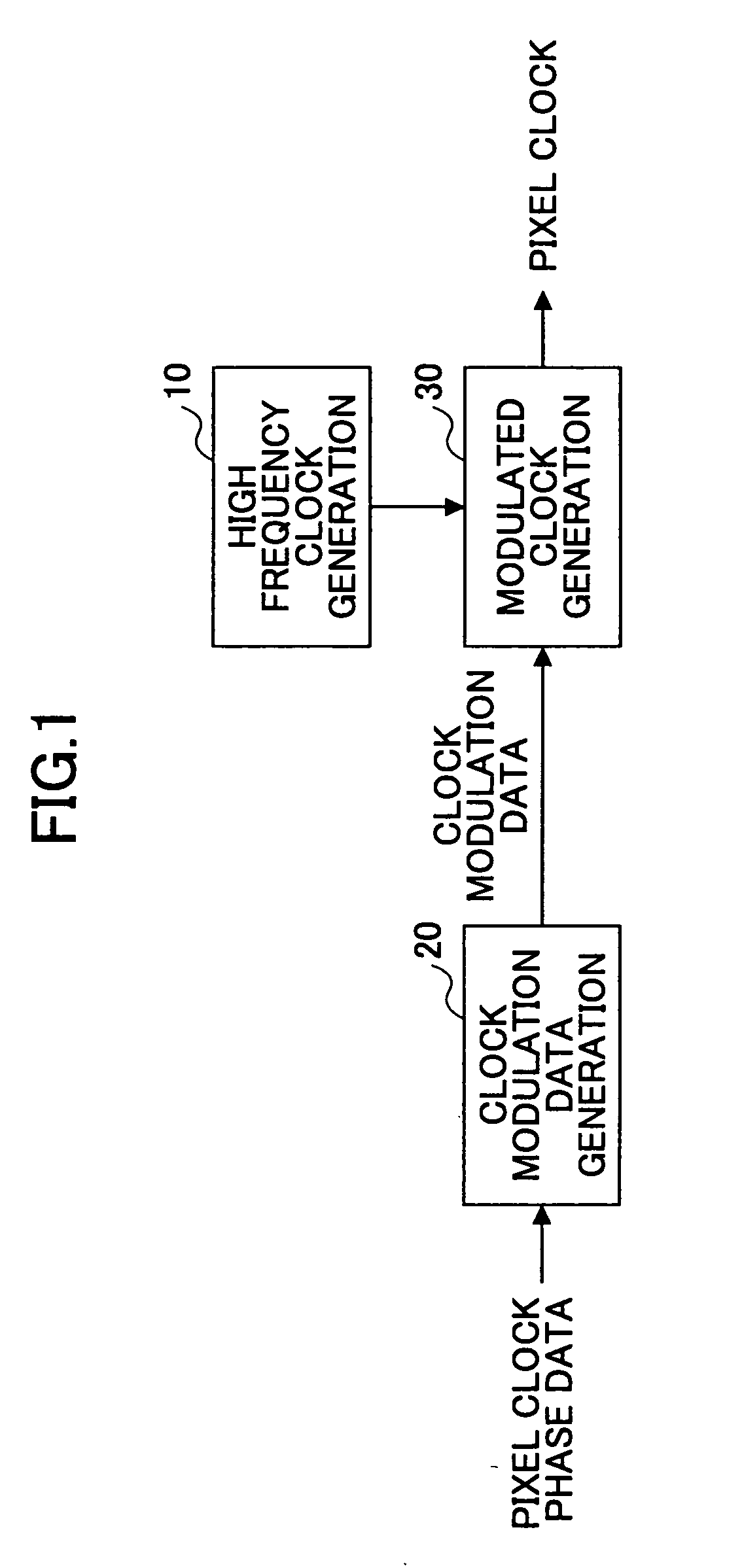
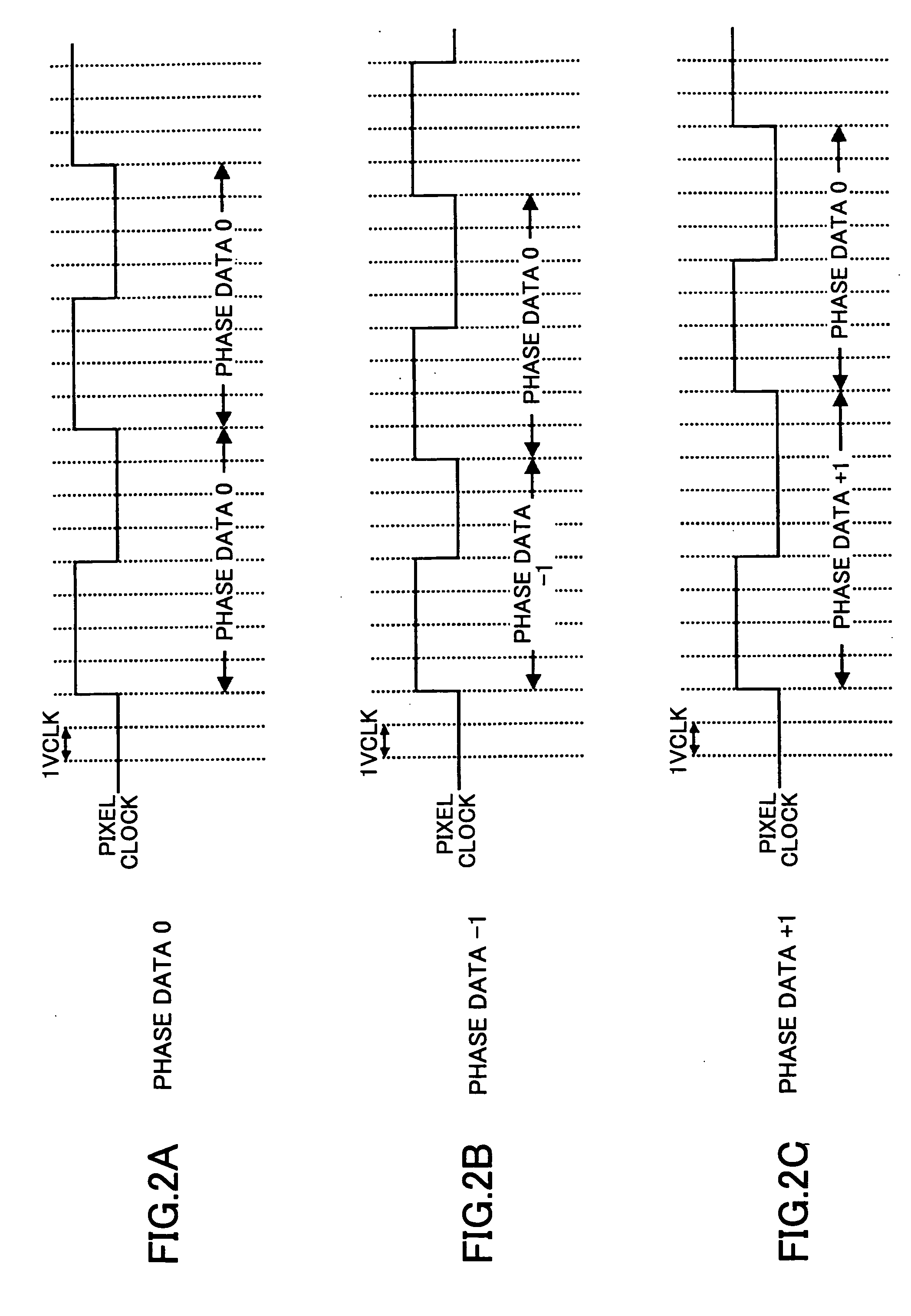
[0056]FIG. 1 illustrates the basic concept of a pixel clock generation circuit according to the present invention. In FIG. 1, a high frequency clock generation unit 10 generates high frequency clock VCLK the frequency is much more higher than that of the pixel clock corresponding to one dot. A clock (CLK) modulation data generation unit 20 generates clock modulation data including consecutive 1's and consecutive 0's, the number of which is variable, based on the pixel clock phase data indicating the timing in which the pixel clock make a transition. A modulation clock generation unit 30 receives (loads) the clock modulation data output by the clock modulation data generation unit 20, and shift the received clock modulation data based on the high frequency clock VCLK, thereby to output pixel clock (modulated pixel clock) the frequency and phase of which are modulate...


PUM


Abstract

A pixel clock generation circuit is disclosed, including a high frequency clock generation unit configured to generate high frequency clock, a clock modulation data generation unit configured to generate clock modulation data based on pixel clock phase data indicating timing of a transition in pixel clock. The pixel clock generation circuit further includes a modulation clock generation unit configured to modulate the frequency and phase of the high frequency clock based on the modulation data thereby to generate modulated pixel clock.

Description

BACKGROUND OF THE INVENTION [0001] 1. Field of the Invention [0002] The present invention generally relates to the generation of pixel clock and phase control thereof used for image forming apparatuses, and particularly, to a pixel clock generation circuit that realizes highly accurate phase control of the pixel clock and a image forming apparatus using the same. [0003] 2. Description of the Related Art [0004] The general construction of an image forming apparatus such as a laser printer and a digital copier is shown in FIG. 40. As shown in FIG. 40, a laser beam emitted by a semiconductor laser unit 4001 is scanned by a rotating polygon mirror 4002, converges into a light spot on a photosensitive unit 4004 via a scan lens 4003, and exposes the photosensitive unit 4004 thereby to form a electrostatic latent image. Each scanned laser beam is detected by a photo detector 4005. A clock generation circuit 4008 provides clock to a phase sync circuit 4009, and the phase sync circuit 4009 g...

Claims


Application Information

Patent Timeline
IPC IPC(8): B41J2/44B41J27/00G06F1/06H03L7/07H03L7/081H03L7/099H04N1/036H04N1/053H04N1/113H04N1/12H04N1/191
CPCH03L7/07H03L7/0812H04N2201/04781H04N2201/0471H04N1/1911H04N1/12H04N1/1135H03L7/0995H04N1/053H04N2201/04732H04N2201/04744H04N2201/02439H04N2201/04794H03L7/0814
Inventor OZASA, DANISHIDA, MASAAKI
Owner RICOH KK
Why Eureka
Try Eureka