
Memory cell for storing an information item, memory circuit and method for producing a memory cell

a memory cell and information item technology, applied in the field of memory cells for storing information items, memory circuits and methods for producing memory cells, can solve the problems of inadvertent cell switching, large area requirements, and high rc time constants for the detection of high-resistance states, and achieve less degradation effects, less noise or signal crosstalk, and read more simply

Inactive Publication Date: 2005-11-03
POLARIS INNOVATIONS
View PDF4 Cites 21 Cited by
  • Summary
  • Abstract
  • Description
  • Claims
  • Application Information

AI Technical Summary

Benefits of technology

[0011] One aspect of the present invention provides an improved memory cell having a PMC resistance component. The memory cell is less sensitive to noise or signal crosstalk, has fewer degradation effects and can be read more simply.
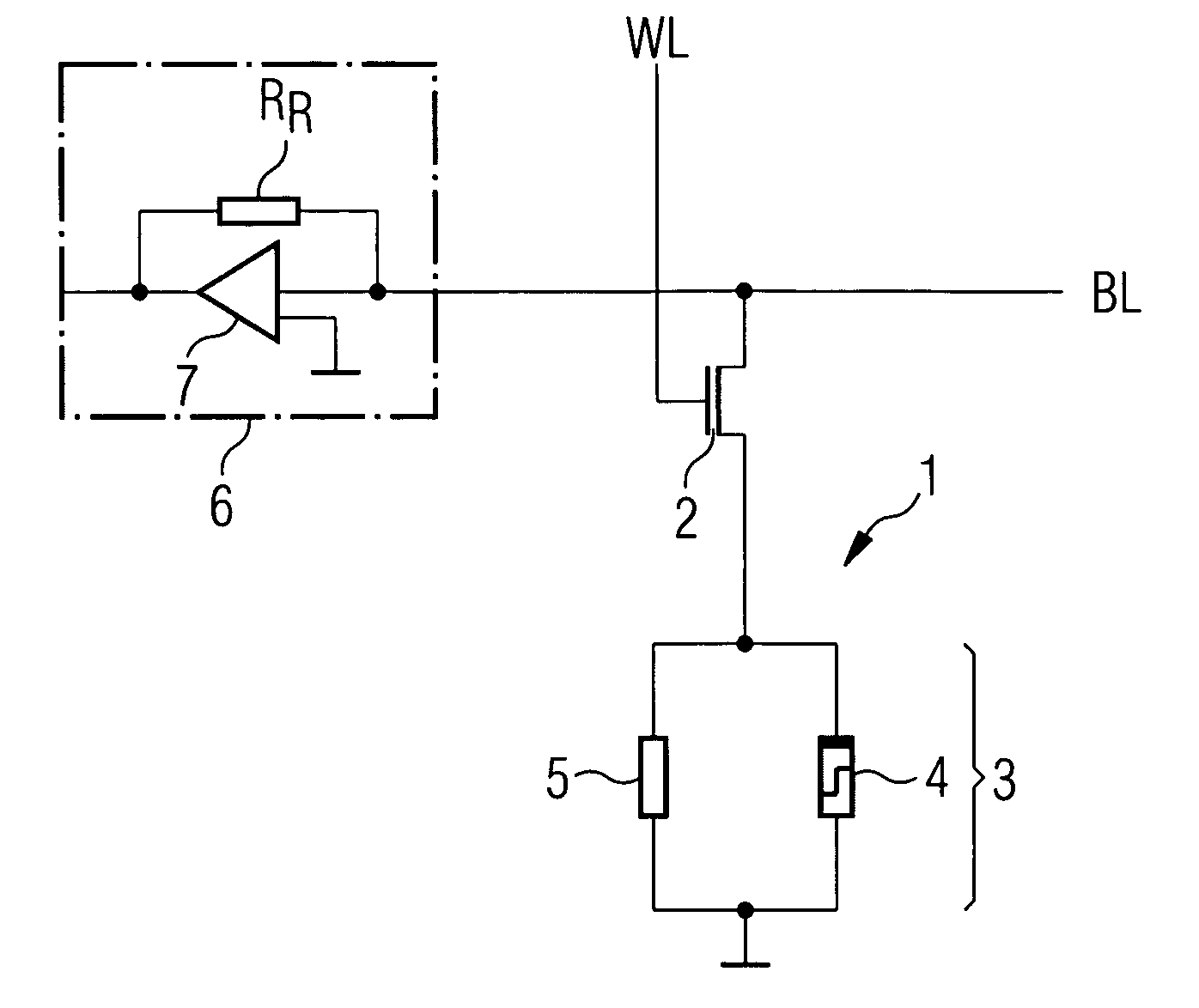
[0013] A first aspect of the present invention provides a memory cell for providing an information item, having a memory element. The memory element comprises a PMC resistance component with a solid electrolyte material, wherein the solid electrolyte material may be put into a first state with a high electrical resistance and into a second state with a low electrical resistance. The memory element further includes a resistance element which is connected to the PMC resistance component in such a way as to reduce the total resistance of the memory element in the first state.
[0014] In the first state, the cell is not electrically insulated from other potential lines of the memory circuit, and the cell thus becomes more sensitive to noise and signal crosstalk on account of instances of capacitive coupling. With regard to a read-out circuit to be provided, an operational amplifier with feedback resistor provided in the read-out circuit can be implemented more simply since the feedback resistor is adapted to the resistance of the memory element for optimum discrimination, and is thus significantly smaller than in the case of a pure PMC resistance component as memory element, which has a high resistance in the first state. The area requirement of such a feedback resistor can thereby be reduced. Moreover, the high RC time constant in the detection of the high-resistance state of the memory element may be reduced since the memory element has a lower resistance.
[0019] A further aspect of the present invention provides a memory circuit having a memory cell as described above. The memory cell is coupled to a read-out circuit to detect the state of the solid electrolyte material, the read-out circuit having a differential amplifier, which is provided with a feedback resistor set to the resistance of the memory element. The adapted feedback resistor may serve to achieve good discrimination between the first and second states.

Problems solved by technology

However, in the realization of a memory cell array with evaluation and drive circuits, a number of disadvantages are associated with the above mentioned resistance values.
Cells in a cell array which are electrically insulated from a defined electrical potential such as the bit / word or plate lines (e.g., by means of the turned-off selection transistor or the extremely high-value resistance of the cell) are therefore very sensitive to noise which, when coupled in, may lead to inadvertent switching of the cell.
High resistance values result in this case and require a large area requirement, particularly when such a memory cell is realized using CMOS technology.
Furthermore, the high resistance values result in high RC time constants and very low current values for the detection of the high-resistance state.
Moreover, the cells exhibit degradation with regard to the high-resistance state over the service life, particularly under stress conditions, such as in the case of many read-in / read-out operations.
The degradation is manifested in a reduction of the resistance value in the high-resistance state and signifies an undesirable inhomogeneity of the cell properties in a memory cell array.

Method used


Image

  • Memory cell for storing an information item, memory circuit and method for producing a memory cell
  • Memory cell for storing an information item, memory circuit and method for producing a memory cell
  • Memory cell for storing an information item, memory circuit and method for producing a memory cell

Examples


Embodiment Construction

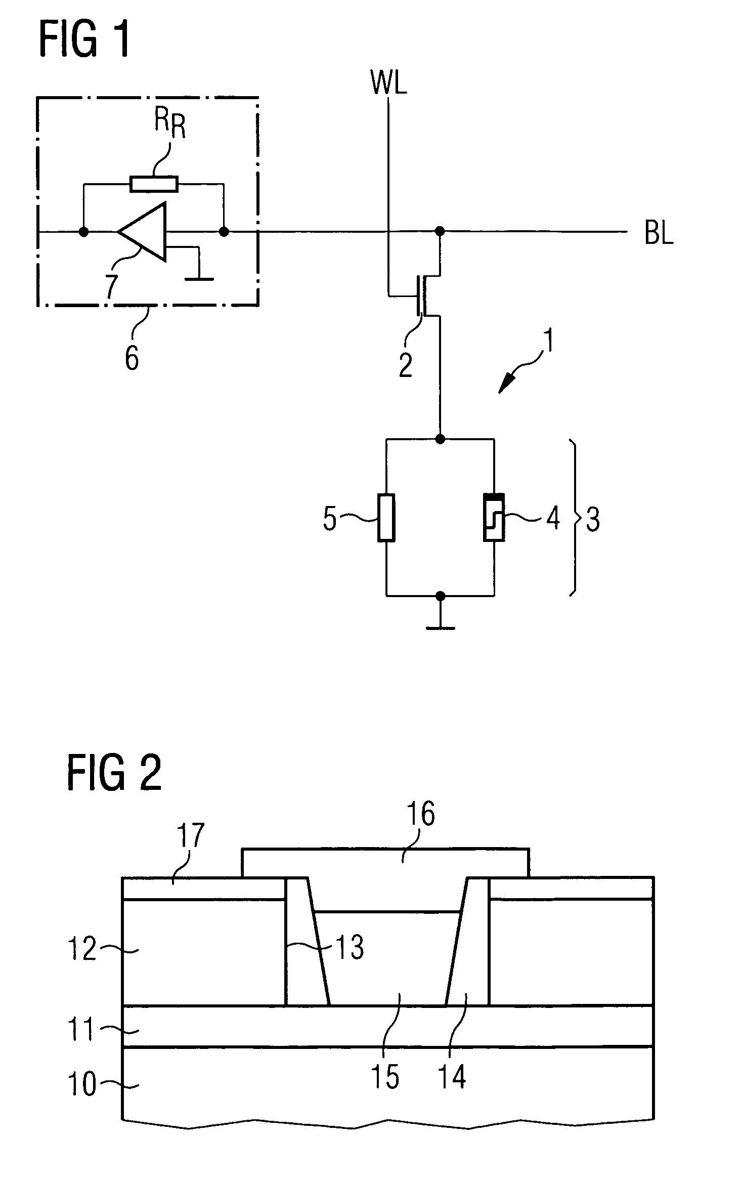
[0030]FIG. 1 shows a circuit diagram of a memory cell 1 according to one embodiment of the invention arranged on a word line WL and on a bit line BL of a memory cell array having a plurality of word lines and a plurality of bit lines (not shown). The word line serves for selecting one of the memory cells on a specific bit line BL, so that the content of the memory cell situated on the activated word line can be read out via the bit line BL. For this purpose, the word line WL is connected to a control terminal of a switch 2 of the memory cell 1. The switch 2 of the memory cell 1 is usually formed by a field effect transistor, the word line WL being connected to the gate terminal of the field effect transistor. A first terminal, e.g., the drain terminal, of the field effect transistor is connected to the bit line, and a second terminal, e.g., the source terminal, is connected to a terminal of the memory element 3.

[0031] The memory element 3 has a PMC resistance component 4, which has...


PUM


Abstract

The invention relates to a memory cell for providing an information item, having a memory element, which has a PMC resistance component with a solid electrolyte material. The solid electrolyte material may be put into a first state with a high electrical resistance and into a second state with a low electrical resistance. The memory element has a resistance element which is connected up to the PMC resistance component in such a way as to reduce the total resistance of the memory element in the first state.

Description

CROSS-REFERENCE TO RELATED APPLICATIONS [0001] This application claims foreign priority benefits under 35 U.S.C. §119 to co-pending German patent application number DE 10 2004 018 715.0, filed 17 Apr. 2004. This related patent application is herein incorporated by reference in its entirety. BACKGROUND OF THE INVENTION [0002] 1. Field of the Invention [0003] The invention relates to a memory cell for providing an information item having a programmable metallization cell (PMC) resistance component. The invention furthermore relates to a memory circuit having such a memory cell and to a method for producing a memory cell having a PMC resistance component. [0004] 2. Description of the Related Art [0005] Semiconductor memory cells based on PMC resistance components are generally known. A PMC resistance component has a solid electrolyte material in which a conductive path can optionally be formed or withdrawn to assume a high-resistance or a low-resistance state that can be assigned to a ...

Claims


Application Information

Patent Timeline
IPC IPC(8): G11C11/00G11C16/00H01L45/00
CPCH01L45/085H01L45/12H01L45/1683H01L45/142H01L45/143H01L45/1233H10N70/245H10N70/801H10N70/8822H10N70/8825H10N70/826H10N70/066
Inventor SYMANCZYK, RALF
Owner POLARIS INNOVATIONS
Learn More