Method for manufacturing display device, liquid crystal telvision, and EL television

a display device and liquid crystal technology, applied in the direction of organic semiconductor devices, instruments, optics, etc., can solve the problems of reducing yield, wasting most of resist materials, reducing throughput, etc., and achieves low wettability, high yield, and high wettability.

Inactive Publication Date: 2005-11-03
SEMICON ENERGY LAB CO LTD
View PDF33 Cites 31 Cited by
  • Summary
  • Abstract
  • Description
  • Claims
  • Application Information

AI Technical Summary

Benefits of technology

[0030] According to the invention, a second mask pattern can be formed in a self-aligned manner without using a photomask by forming the second mask pattern of a material having high wettability using as a mask a first mask pattern formed of a material having low wettability by a droplet discharge method, an ink-jet method, a printing method, or the like. Therefore, a mask pattern can be formed without requiring a plurality of times of light exposure by forming a mask pattern using materials having different wettability over a large-sized substrate. In the case of using a large-sized substrate, unconformity is not generated among adjacent patterns, thereby increasing yield.
[0031] A pixel electrode or a display device having a pixel electrode can be formed with high yield by forming the second mask pattern over a conductive layer and etching the conductive layer.
[0032] A first mask pattern can be formed using a droplet discharge method by discharging a droplet to a predetermined position by changing a relative position of a substrate and a nozzle that is a discharge opening of a droplet including a material of the first mask pattern. A thickness and a width of a pattern to be formed can be adjusted depending on a nozzle diameter, the discharge amount of droplets, and a relative relationship between movement speed of a nozzle and that of a substrate to be provided with a discharged droplet. Accordingly, a mask pattern can be formed by discharging in a desired portion with high accuracy even over a large-sized substrate having a side of 1 m to 2 m or more. Thus, a display device can be manufactured with few steps and high yield. Further, cost can also be reduced.
[0033] Further, a liquid crystal television or an EL television having the display device formed according to the above-described manufacturing step can be manufactured at low cost with high throughput and yield.

Problems solved by technology

However, since a resist that is a material of a mask pattern is applied to a substrate using a spin coating method in a conventional step of forming a film pattern using a photolithography step, there is a problem of wasting most of a resist material as well as reducing throughput due to a number of steps of forming a mask pattern.
A light exposure apparatus used for the photolithography step has difficulty in performing light exposure treatment on a large-sized substrate at a time.
Therefore, a method for manufacturing an active matrix substrate of a display device using a large-sized substrate has a problem of needing to perform light exposure plural times and generating unconformity among adjacent patterns, thereby reducing yield.

Method used


Image

  • Method for manufacturing display device, liquid crystal telvision, and EL television
  • Method for manufacturing display device, liquid crystal telvision, and EL television
  • Method for manufacturing display device, liquid crystal telvision, and EL television

Examples


embodiment mode 1

(Embodiment Mode 1)

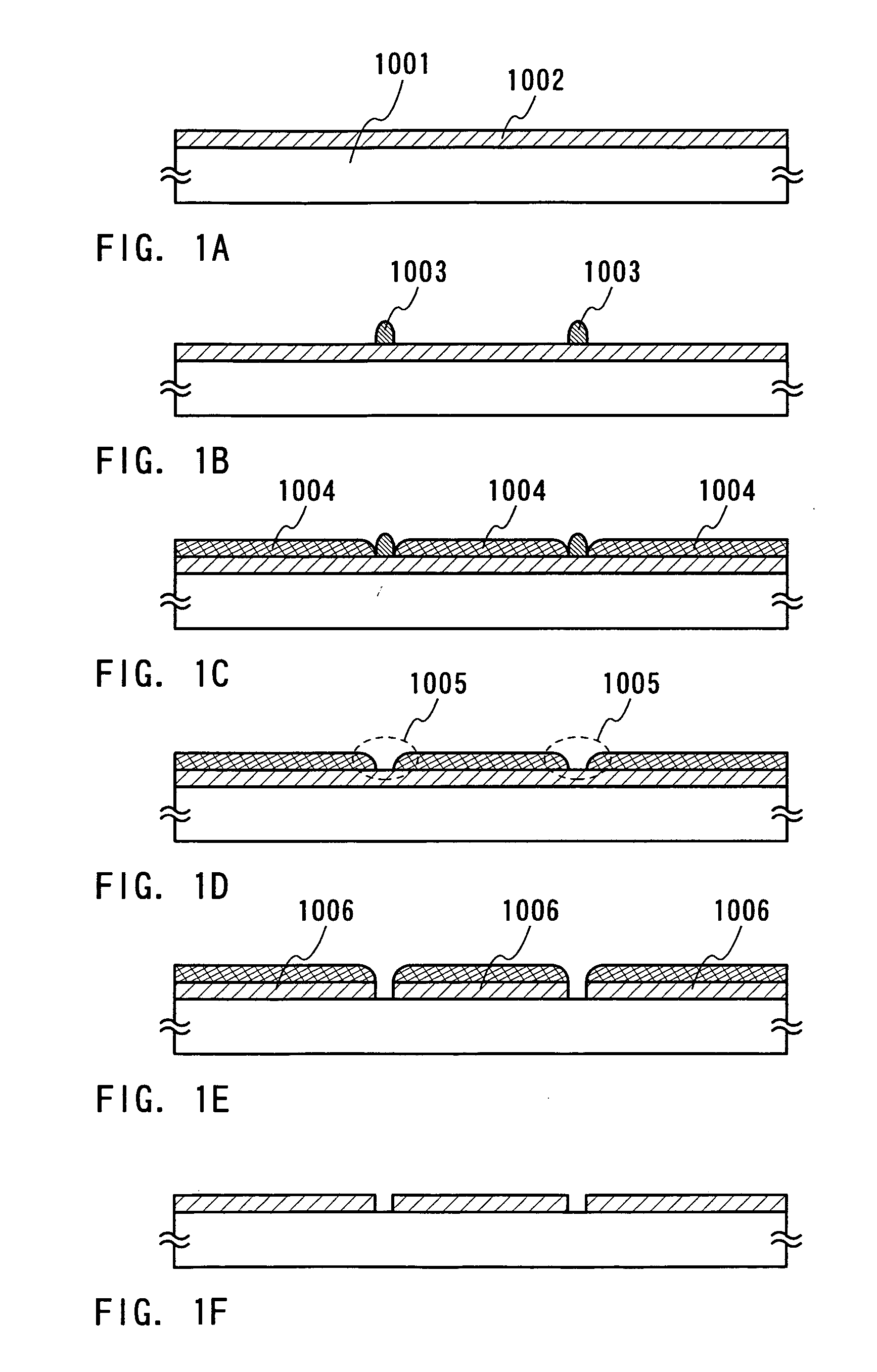
[0062] This embodiment mode describes, with reference to FIGS. 1A to 1F, a step of forming a mask pattern for forming a pixel electrode by forming a first mask pattern of a material having low wettability over a conductive film, forming a second mask pattern of a material having high wettability, and removing the first mask pattern and a step of forming a pixel electrode.

[0063] A first conductive layer 1002 is formed over a substrate 1001 as shown in FIG. 1A. The first conductive layer is formed of a conductive material which can serve as a pixel electrode.

[0064] A glass substrate, a quartz substrate, a substrate formed of an insulating material such as alumina, a heat-resistant plastic substrate which can withstand a processing temperature of a later step, a silicon wafer, a metal plate, or the like can be typically used as the substrate 1001. In this case, an insulating film for preventing impurities from the substrate side from diffusing, such as a silicon ox...

embodiment mode 2

(Embodiment Mode 2)

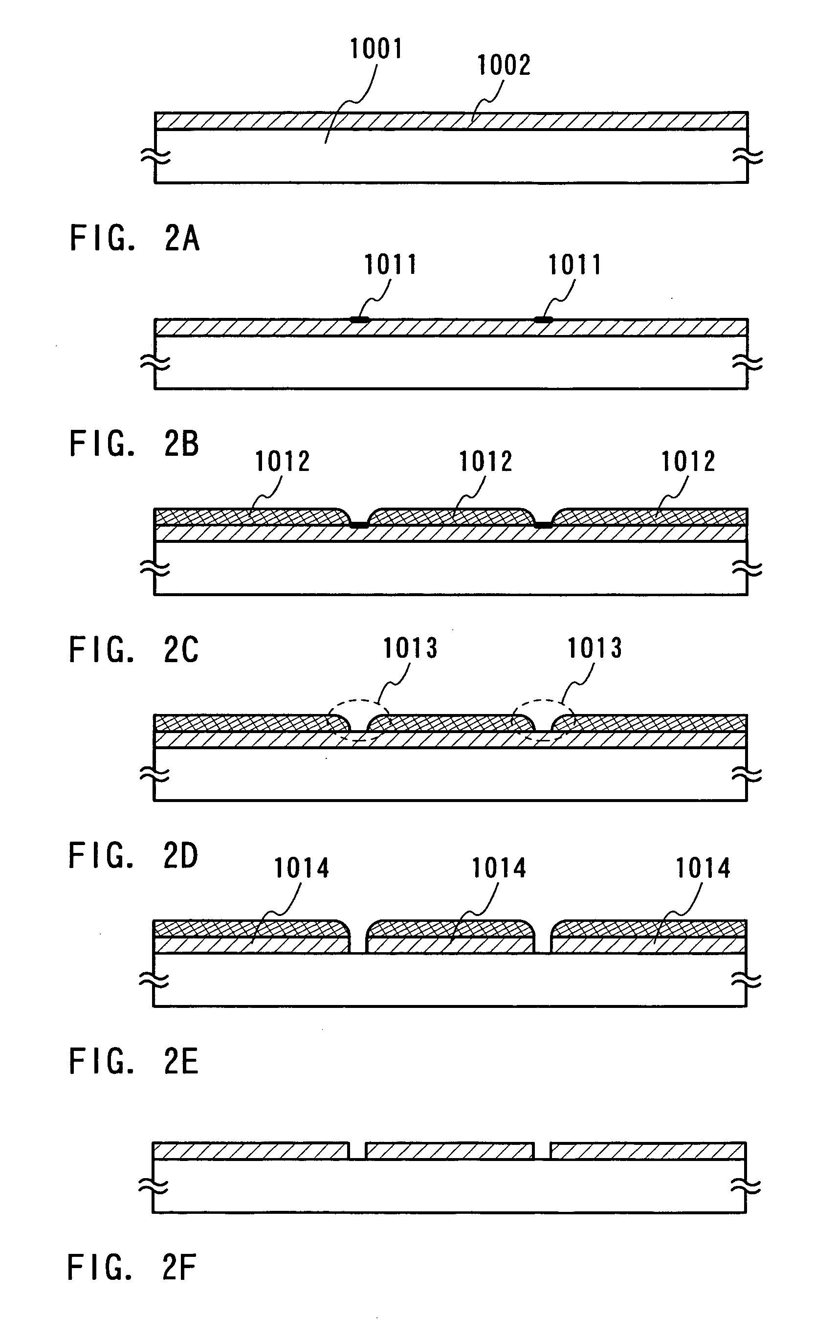
[0083] This embodiment mode describes, with reference to FIGS. 2A to 2F, a step of forming a mask pattern for forming a pixel electrode by forming a first mask pattern using a material having low wettability with the use of a compound including a fluorocarbon chain and then forming a second mask pattern using a material having high wettability and a step of forming a pixel electrode.

[0084] As in Embodiment Mode 1, a first conductive layer 1002 is formed over a substrate 1001 as shown in FIG. 2A.

[0085] Afirst mask pattern 1011 is formed over the first conductive layer 1002 as shown in FIG. 2B. In this embodiment mode, a mask pattern having low wettability is formed as the first mask pattern. A material having low wettability is applied by a printing method typified by screen (stencil) printing, offset (planographic) printing, relief printing, gravure (intaglio) printing, or the like, a droplet discharge method, or the like to form the first mask pattern 1011. A s...

embodiment mode 3

(Embodiment Mode 3)

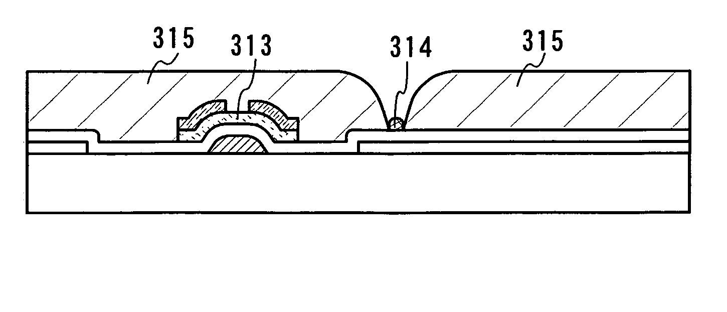
[0095] This embodiment mode describes a method for manufacturing an active matrix substrate of a display device with reference to FIGS. 3A to 3F. This embodiment mode is described using a bottom gate channel etch TFT as a pixel driving element. Note that a second conductive layer 301 is formed using Embodiment Mode 1; however, this embodiment mode is not limited thereto. Embodiment Mode 2 can also be used.

[0096] A first conductive layer 1002 is formed over a substrate 1001 as shown in FIG. 3A. After a first mask pattern 1003 is formed according to a similar step to that in Embodiment Mode 1, a second mask pattern 1004 is formed.

[0097] The first mask pattern 1003 is removed to expose a portion of the first conductive layer. The first conductive layer is etched to form the second conductive layer 301 serving as a pixel electrode. Then, the second mask pattern 1004 is removed.

[0098] A third conductive layer 302 serving as a gate electrode is formed over the substr...


PUM

PropertyMeasurementUnit
contact angleaaaaaaaaaa
diameteraaaaaaaaaa

Abstract

An object of the present invention is to provide a method for manufacturing a display device with few steps and high yield. One feature of the invention is to form a first mask pattern having low wettability over a conductive layer, form a second mask pattern having high wettability over the conductive layer using the first mask pattern as a mask, and form a mask pattern for etching the conductive layer by removing the first mask pattern. Another feature is to form a pixel electrode by etching the conductive layer.

Description

BACKGROUND OF THE INVENTION [0001] 1. Field of the Invention [0002] The invention relates to a display device having a pixel electrode formed by a droplet discharge method typified by an ink-jet method, and a manufacturing method thereof. [0003] 2. Description of the Related Art [0004] A so-called active matrix drive display panel including a semiconductor element typified by a thin film transistor (hereinafter also referred to as a “TFT”) over a glass substrate is manufactured by patterning according to a light exposure step using a photomask (hereinafter referred to as a photolithography step) and etching various thin films. [0005] In the photolithography step, a resist pattern is formed by coating an entire surface of a substrate with a resist, prebaking, irradiating with ultraviolet light or the like with a photomask therebetween, and then developing. Thereafter, a film pattern of a semiconductor region, an electrode, a wiring, or the like is formed by etching and removing a thi...

Claims


Application Information

Patent Timeline
Patent Type & Authority Applications(United States)
IPC IPC(8): G02F1/1343H01L21/768H01L21/77H01L21/84H01L27/32H01L51/56
CPCG02F1/13439H01L27/3244H01L27/3297H01L27/1292H01L2251/5315H01L2251/5323H01L51/56H10K59/12H10K59/123H10K59/131H10K71/621H10K2102/3026H10K2102/3031H10K71/00H10K59/805
Inventor FUKUCHI, KUNIHIKOISA, TOSHIYUKIFUJII, GEN
Owner SEMICON ENERGY LAB CO LTD
Why Eureka
Try Eureka