Semiconductor device having a gettering layer

a technology of semiconductor chips and gettering layers, which is applied in the direction of semiconductor devices, basic electric elements, electrical appliances, etc., can solve the problems of reducing the mechanical strength affecting the performance of the semiconductor chip, and mixing of incoming heavy metals, etc., to achieve superior transistor characteristics, high rigidity, and sufficient mechanical strength

Inactive Publication Date: 2005-11-03
ELPIDA MEMORY INC
View PDF5 Cites 5 Cited by
  • Summary
  • Abstract
  • Description
  • Claims
  • Application Information

AI Technical Summary

Benefits of technology

[0022] In accordance with the semiconductor device of the present invention and a semiconductor device manufactured by the method of the present invention, since the thickness of the impurity-doped layer having a high rigidity is not less than 50% of the thickness of the semiconductor substrate, the resultant semiconductor device has a sufficient mechanical strength even if the semiconductor substrate has a thickness not larger than 130 μm. In addition, since the gettering function of the impurity-doped layer prevents heavy metals from diffusing from the bottom surface of the substrate toward the vicinity of the semiconductor active layer, the resultant semiconductor device has superior transistor characteristics.

Problems solved by technology

Any semiconductor device provided in the form of a semiconductor chip generally has a problem in that incoming heavy metals mixed in the semiconductor substrate or attached onto the surfaces of the device diffuse to the vicinity of the element active region during heat treatments performed in the process of manufacturing the semiconductor device.
The thickness of the MCP module is particularly limited, depending on its specification.
If a semiconductor substrate is polished to thickness of 300 μm or less, however, the mechanical strength of the semiconductor chip will decrease.
The decrease of mechanical strength results partly from a damage caused by the polishing applied onto the bottom surface of the semiconductor substrate.
The semiconductor chip having such a polishing damage may be broken when it receives even a small external impact.
These findings reveal that practical usage of semiconductor devices that have a substrate thickness of about 100 μm or less encounters a large obstacle.
It was also found that the decrease in the reliability of the semiconductor device due to the mirror-polishing treatment results from an increase in the amount of heavy metals that diffuse into the vicinity of the element active region, after the polishing damage having a gettering function is eliminated.
The heavy metals thus trapped have an energy level in the bandgap energy and may become a source of leakage current.
In this case, however, crystal defects will grow due to the oxygen precipitation as well as due to the conditions of heat treatment, resulting in crystal dislocation.
Once crystal dislocation occurs, a large number of voids in the dislocation inevitably promote the diffusion of heavy metals.
As described above, it is difficult to use the gettering layer, that is an oxygen-precipitated layer, due to the difficulty of controlling the oxygen concentration during growth of silicon and the conditions of heat treatment.
The gettering layer has only a limited gettering efficiency.
Further, the thickness thereof is limited in a semiconductor device having a small-thickness substrate.
The gettering layer alone can hardly control the diffusion of heavy metals.

Method used


Image

  • Semiconductor device having a gettering layer
  • Semiconductor device having a gettering layer
  • Semiconductor device having a gettering layer

Examples


Embodiment Construction

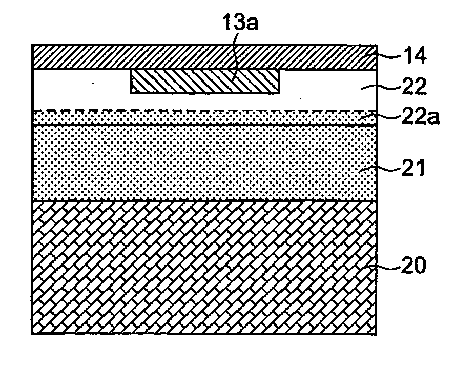
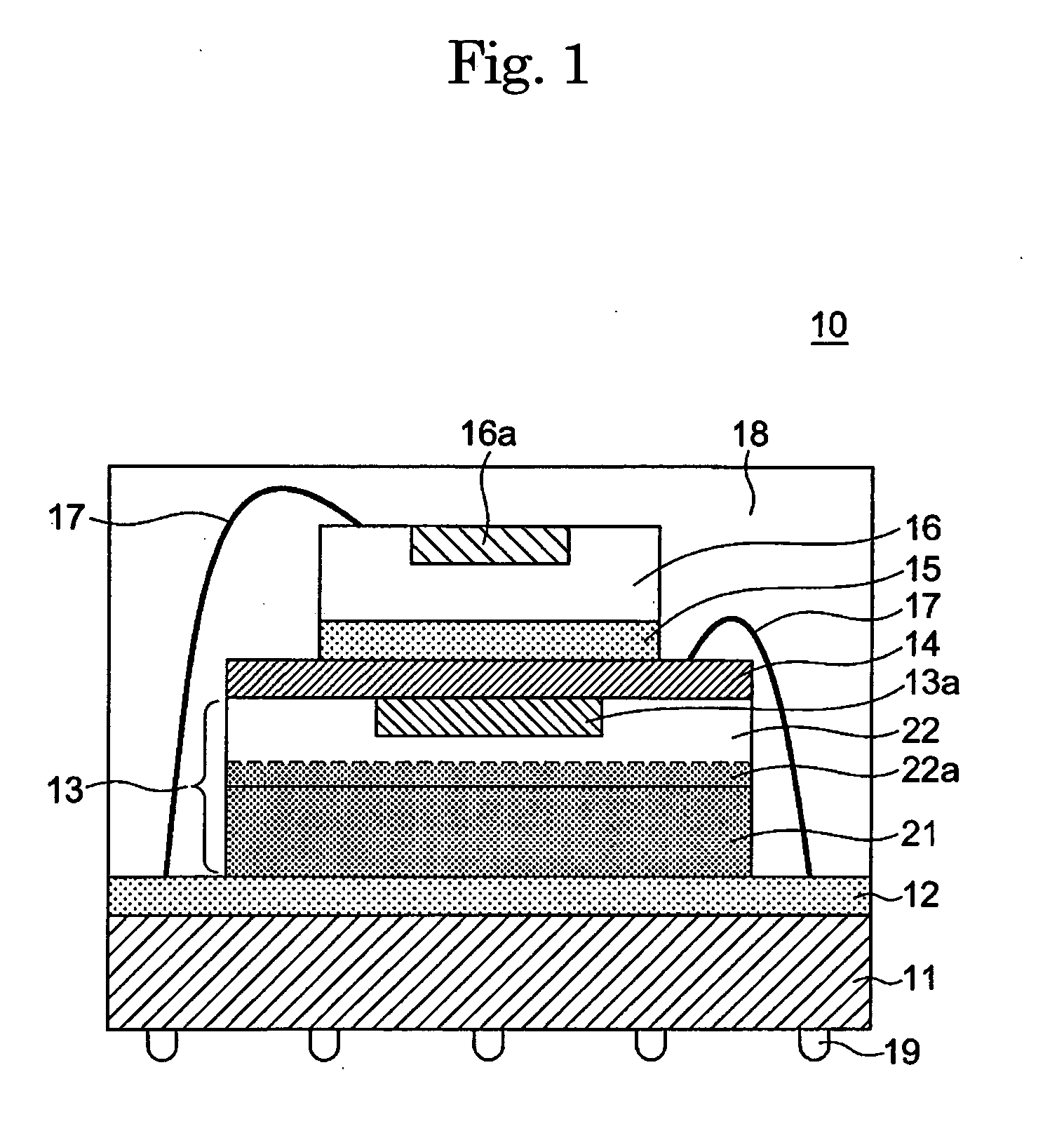
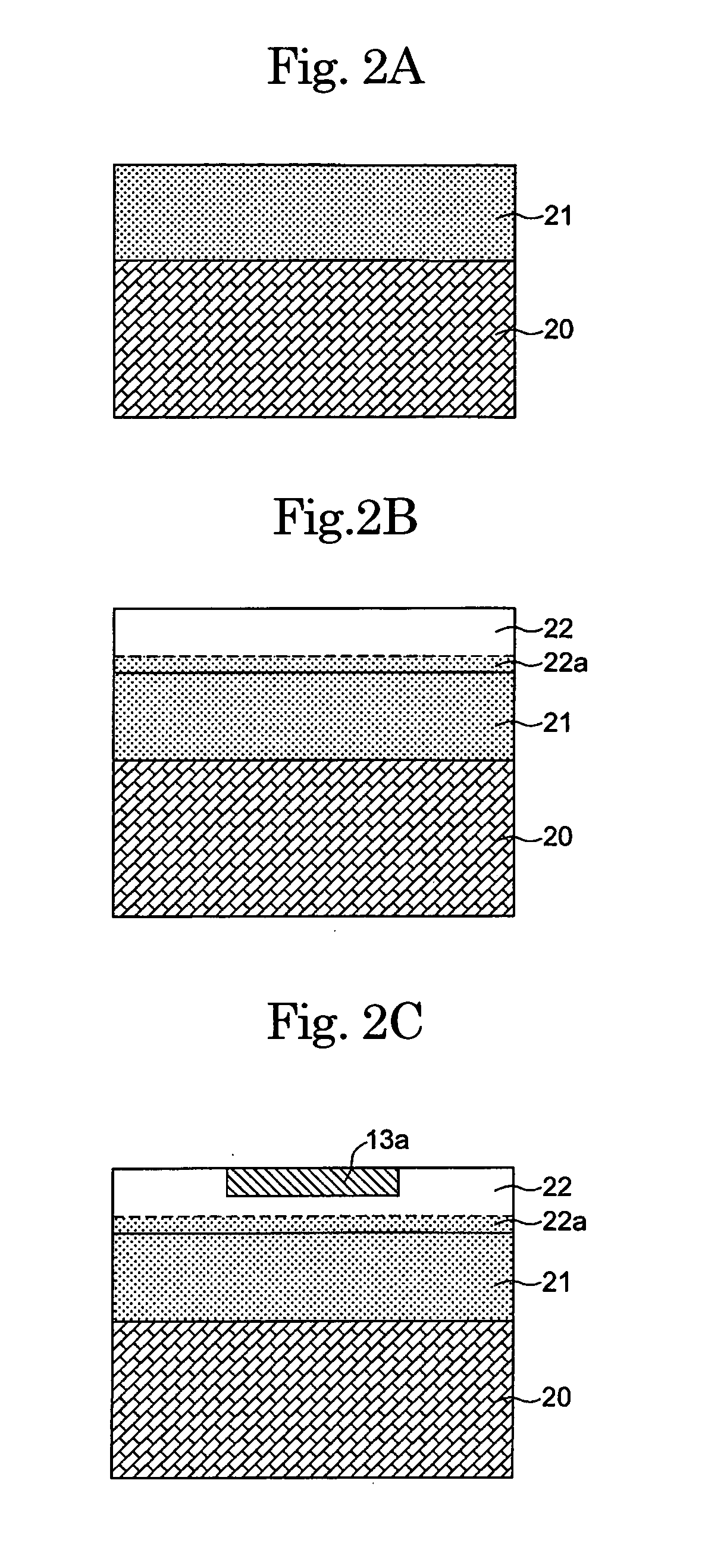
[0032] Before achieving the present invention, the inventor conducted two experiments in order to study the problem that the reliability of semiconductor devices decreases due to the reduction in thickness and the mirror-polishing treatment of the bottom surface of the substrate. In the first experiment, three types of the lower semiconductor chips were fabricated for use in the MCP module 30 shown in FIG. 5. More specifically, several chips of each type were manufactured as the samples for experiments. Each lower semiconductor chip of the samples-1 had a substrate which was 120 a m thick, the bottom surface of the substrate being subjected to a rough polishing treatment. Each lower semiconductor chip of the samsples-2 had a substrate which was 120 μm thick, the bottom surface of the substrate being subjected to both rough polishing and mirror-polishing treatments. Each lower semiconductor chip of the samples-3 had a substrate which was 100 am thick, the bottom surface of the substr...


PUM


Abstract

A multi-chip-package (MCP) module includes a plurality of semiconductor chips layered one on another. The lower semiconductor chip includes a semiconductor substrate having a top active layer and a bottom heavily-doped layer. The bottom of the heavily-doped layer is polished twice by a rough-polishing treatment and a mirror-polishing treatment. The thickness of the impurity-doped layer is not less than 50% of the thickness of the semiconductor substrate which is not larger than 130 μm.

Description

BACKGROUND OF THE INVENTION [0001] 1. Field of the Invention [0002] The present invention relates to a semiconductor device having a gettering layer and a method for manufacturing the same. More particularly, the present invention relates to a semiconductor device having a gettering layer in a small-thickness substrate for use as a semiconductor chip in a multi-chip-package (MCP) system, and also to a method for manufacturing such a semiconductor device. [0003] 2. Description of the Related Art [0004] Any semiconductor device provided in the form of a semiconductor chip generally has a problem in that incoming heavy metals mixed in the semiconductor substrate or attached onto the surfaces of the device diffuse to the vicinity of the element active region during heat treatments performed in the process of manufacturing the semiconductor device. To suppress the degradation in the reliability of the semiconductor device caused by the heavy metals, a variety of measures have been employ...

Claims


Application Information

Patent Timeline
Patent Type & Authority Applications(United States)
IPC IPC(8): H01L25/18H01L21/30H01L21/322H01L21/44H01L21/48H01L25/065H01L25/07
CPCH01L21/3221H01L25/0657H01L2224/32145H01L2224/32225H01L2924/01019H01L2224/48227H01L2224/73265H01L2924/15311H01L2224/48091H01L2924/00014H01L2924/00H01L2924/00012H01L24/73
Inventor INOUE, YASUKAZU
Owner ELPIDA MEMORY INC
Why Eureka
Try Eureka