Display device and projection type display apparatus

a display device and display device technology, applied in projectors, instruments, computing, etc., can solve the problems of short time which can be spent on writing to each pixel, high drive frequency, and considerable frequency, so as to improve picture quality, prevent the degradation of picture quality caused by the delay of scanning timing, and improve picture quality

Inactive Publication Date: 2005-11-10
SONY CORP
View PDF6 Cites 36 Cited by
  • Summary
  • Abstract
  • Description
  • Claims
  • Application Information

AI Technical Summary

Benefits of technology

[0047] Accordingly, since the difference in intensity and so on are not generated in the pixels next to each other with the division boundary line positioned in between, the division boundary line becomes invisible as a joint, so that picture quality can be improved.
[0049] With this, the length of the gate line of each display area becomes half by dividing the display area into two not only in the column direction but also in the row direction, so that the wiring resistance and parasitic capacitance of the gate line can also be made small. Accordingly, since the delay of the scanning timing (the delay of the timing when a switching element of each pixel on the gate line is turned on) caused by the wiring resistance and parasitic capacitance of the gate line can be decreased, the deterioration of the picture quality which is caused by this delay of scanning timing can also be prevented.
[0051] This projection type display apparatus uses the above described display device according to the present invention as an optical modulation device, and since the division boundary line of each display area of an optical modulation device becomes invisible as a joint on a projection screen, a large screen display with the high picture quality is attained.
[0052] According to the present invention, in the display device of the matrix drive method when a display area is divided into two or more areas and those areas are driven independently from each other, the difference in intensity and so on are not generated in the pixels next to each other with the division boundary line of respective display areas positioned in between, so that the division boundary line becomes invisible as a joint and the picture quality can be improved.
[0053] Moreover, since a display area is divided into two not only in the column direction but also in the row direction, the delay of the scanning timing caused by a wiring resistance and parasitic capacitance of the gate line is decreased, so that the degradation of the picture quality caused by the delay of this scanning timing can also be prevented.

Problems solved by technology

On the other hand, in the dot sequential drive method, because the writing to all pixels must be completed in one frame by writing to each pixel one by one (or to a plurality of adjacent pixels as a unit), the time which can be spent on the writing to each pixel becomes short, and the drive frequency becomes high.
When the writing is concerned, there is a period of time at least necessary for writing to the pixel (the time to charge an auxiliary capacitance), and making drive frequency considerably high will cause increase in the burden of a circuit.
Therefore, with the shortened time, there is a limit in the high definition.
However, as for this division drive method, there is a problem of the degradation of the picture quality, because a division boundary line may become visible as a joint when difference of intensity and so on occur in those pixels, in the case where the writing timing to the pixels next to each other with the division boundary line of those display areas positioned in between becomes different.
Further, as also shown in FIG. 4, since the time required for stabilizing the writing voltage becomes long if the degree of the bluntness of the analog waveform becomes large due to the long delay time, the influence of the waveform written in the pixel of the prior stage (for example, in the liquid crystal display device of FIG. 2, pixels of the prior stage to the eight central pixels are the eight pixels on the right side) remains, so that a ghost occurs on a display screen and this also leads to the degradation of picture quality.
As described above, when a display area is divided into a plurality of areas in a display device with considerably a short writing time to a pixel such as a liquid crystal display device of a dot sequential drive method using a single-crystal silicon transistor as a switching element, the delay time until the display data is supplied to pixels of each display area causes the degradation of picture quality.

Method used


Image

  • Display device and projection type display apparatus
  • Display device and projection type display apparatus
  • Display device and projection type display apparatus

Examples


embodiment 1

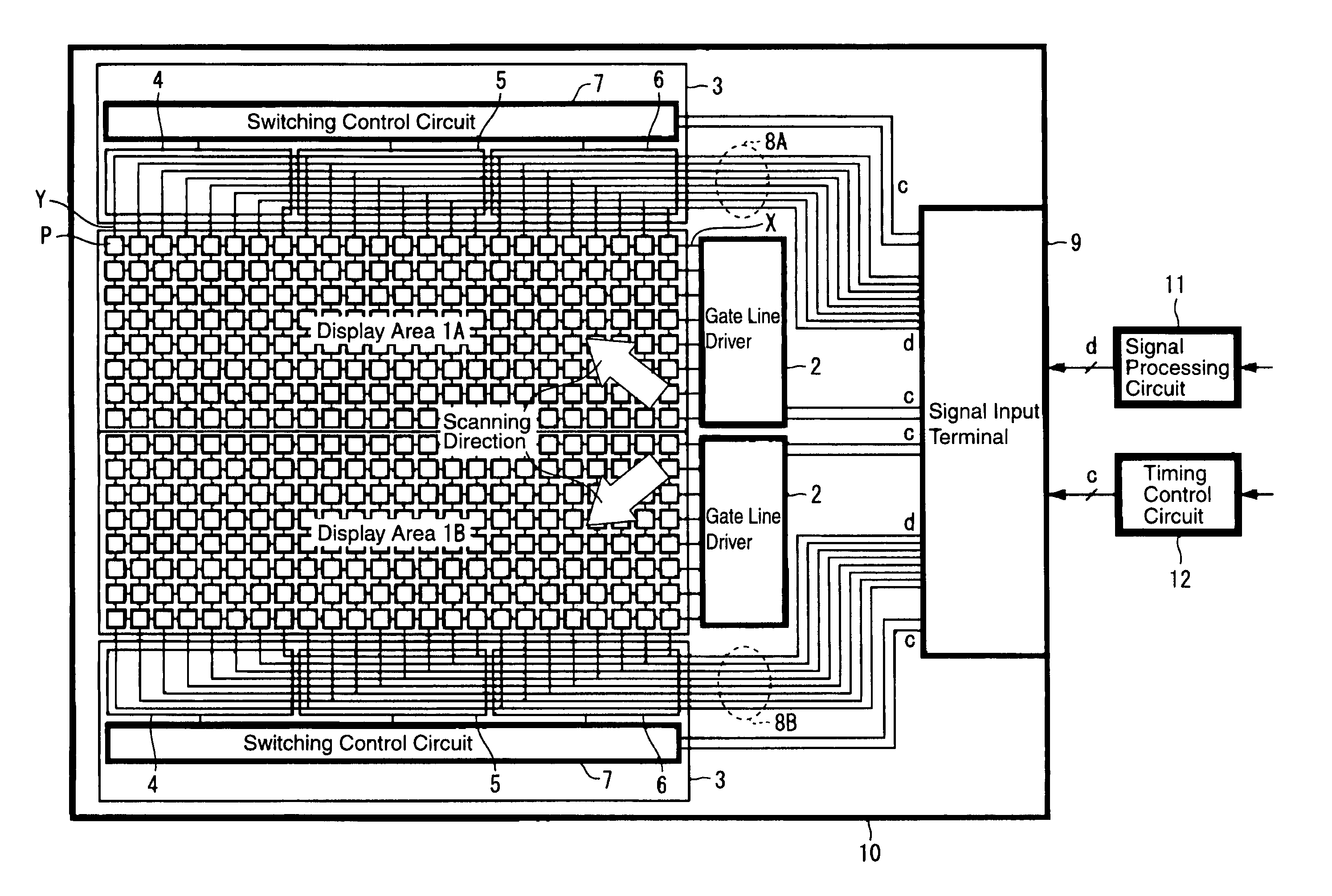
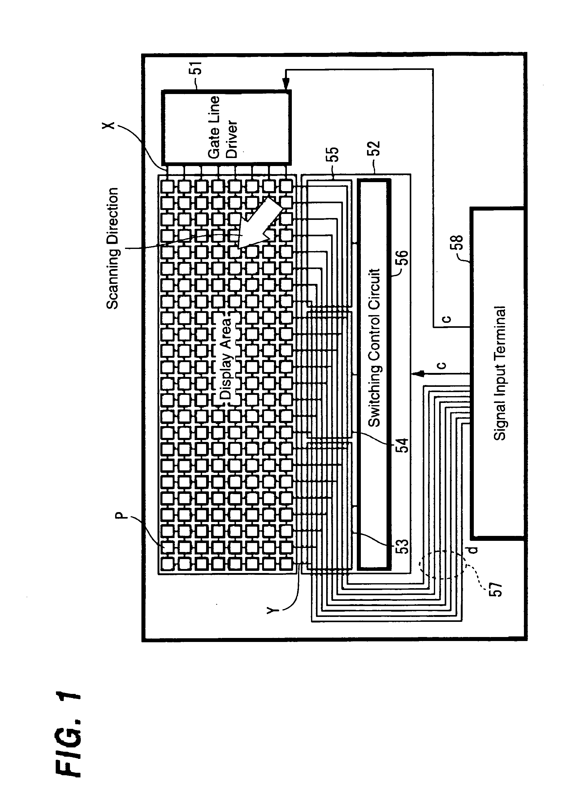
[0067]FIG. 5 shows an example of a configuration of a liquid crystal display device of a dot sequential drive method to which the present invention is applied. This liquid crystal device is a reflective liquid crystal display device in which the liquid crystal is injected between a glass substrate on which the transparent electrode is formed and a drive circuit board (a silicon substrate, for example), and the configuration on the side of the drive circuit board is shown in the figure. A display area on a drive circuit board 10 is divided into two areas 1A and 1B of the top and bottom in the column direction (vertical direction in the drawing).

[0068] Gate lines X in the row direction (horizontal direction in the drawing) and data lines Y in the column direction are arranged in each of areas 1A and 1B in the shape of matrix, respectively. A pixel electrode (a metal mainly composed of aluminum, for example) which applies the voltage and reflects light to a liquid crystal, a single-cr...

embodiment 2

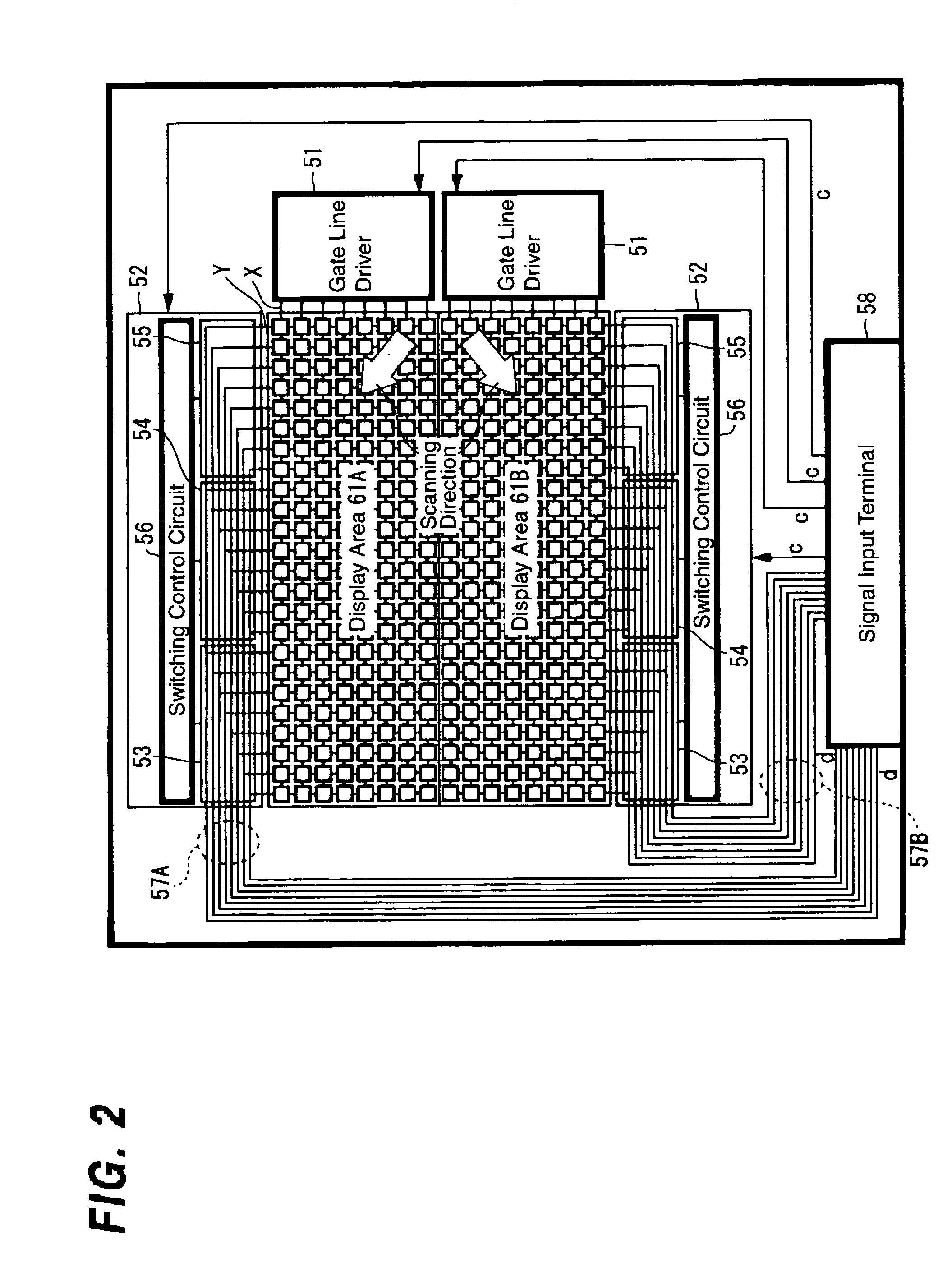
[0102] Next, FIG. 9 shows another example of a configuration of a liquid crystal display device of the dot sequential drive method to which the present invention is applied. this liquid crystal display device is a reflective liquid crystal display device in which the liquid crystal is injected between a glass substrate in which the transparent electrode is formed, and a drive circuit board (for example, a silicon substrate), and a configuration on the side of the drive circuit board is shown in the drawing. On this drive circuit board30, a display area is divided into two of the top and bottom in the column direction (vertical direction in the drawing), and also divided into the right and left areas in the row direction (horizontal direction in the drawing), so that the display area is divided into four areas 21A to 21D.

[0103] The gate lines X in the row direction (horizontal direction in the drawing) and the data lines Y in the column direction are arranged in each of areas 21A to...

embodiment 3

[0151]FIG. 12 shows an example of a configuration of a liquid crystal projector to which the present invention is applied. In this liquid crystal projector, light emitted from an electric discharge lamp 41 which is a light source is made into the parallel light by a reflector 42, and enters a dichroic mirror 44 which reflects blue light through a condenser 43. Red light and green light which have passed through the dichroic mirror 44 are reflected by a mirror 45, and enters a dichroic mirror 46 which reflects green light.

[0152] The red light which has passed through a dichroic mirror 46, the green light reflected by the dichroic mirror 46 and the blue light reflected by the dichroic mirror 44 are input to polarizing beam splitters 47(R), 47(G), and 47(B), respectively. Then, each specific linear polarized light of respective blue light, green light and red light (having either of P polarization or S polarization) is input to reflective liquid crystal display devices 48(R), 48(G) an...


PUM

PropertyMeasurementUnit
delay timeaaaaaaaaaa

Abstract

A display device having extremely short writing time to a pixel such as the liquid crystal display device of a dot sequential drive method using a single-crystal silicon transistor as a switching element is provided in which in the case where a display area is divided into two or more areas, the degradation of picture quality is prevented to perform a high definition display. In a display device of a matrix drive method in which gate lines X in the row direction and data lines Y in the column direction are arranged in matrix shape and a pixel P is arranged at the intersection of the gate line and the data line, a display area is divided into two or more areas 1A and 1B which are driven independently from each other; wiring layout of signal lines 8A and 8B which transfer display data d to each of the areas 1A and 1B is approximately symmetrical with a division boundary line of those areas positioned in between; and control unit 12 which makes a control to perform writing of the display data at least to the pixels P next to each other with the division boundary line positioned in between at approximately the same timing.

Description

BACKGROUND OF THE INVENTION [0001] 1. Field of the Invention [0002] The present invention relates to a display device of a matrix-drive type and a projection type display apparatus (projector system) which employs such display device. [0003] 2. Description of the Related Art [0004] Recently, projector systems which are miniaturized and have a higher definition and a higher intensity have been in great demand. In connection therewith, a display device which is used in a projector system is required to be small-sized and have a high definition, and also is required to have a high efficiency in use of light which comes from a light source. [0005] One of the display devices which satisfy such demand is a reflective liquid crystal display device of the active matrix-drive method. This is the one in which liquid crystal is injected between a glass substrate on which a transparent electrode is formed and a drive circuit board. On the drive circuit board are arranged gate lines in the row d...

Claims


Application Information

Patent Timeline
Patent Type & Authority Applications(United States)
IPC IPC(8): G02F1/13G02F1/133G02F1/1345G02F1/136G02F1/1362G02F1/1368G03B21/00G09G3/20G09G3/36G09G5/00
CPCG02F1/136286G02F2001/133391G09G3/3666G09G2310/0205G09G2320/0252G09G2310/0283G09G2310/0297G09G2320/0233G09G2310/0275G02F1/133391G02F1/133
Inventor YOSHINAGA, TOMOROHASHIMOTO, SHUNICHIAKIMOTO, OSAMUKICHIMI, TOMOAKI
Owner SONY CORP
Why Eureka
Try Eureka