Superconductor fabrication processes

a superconductor and fabrication process technology, applied in the direction of superconductor devices, electric/magnetic/electromagnetic heating, instruments, etc., can solve the problems of numerous engineering and manufacturing challenges, tapes do not represent commercially feasible products, and continue to exis

Inactive Publication Date: 2005-11-10
SUPERPOWER INC
View PDF30 Cites 16 Cited by
  • Summary
  • Abstract
  • Description
  • Claims
  • Application Information

AI Technical Summary

Benefits of technology

[0009] According to an aspect of the present invention, a method of forming a superconductive device is provided including providing a substrate having a dimension ratio of not less than about 102, and depositing a buffer film to overlie the substrate by ion beam assisted deposition utilizing an ion beam. Further, the method calls for monitoring a spatial ion beam density of the ion beam over a target area, and depositing a superconductor layer to overlie the buffer film.
[0010] According to another embodiment, a method for forming a superconductive device is provided, including providing a substrate having a dimension ratio not less than 102, and depositing a buffer film so as to overlie the substrate by ion beam assisted deposition. Further, monitoring an ion beam density is carried out by utilizing an ion detector having an acceptance angle of not less than 10°. The process further calls for depositing a superconducting layer to overlie the buffer film.

Problems solved by technology

However, it was not until somewhat recently that oxide-based high-temperature (high-Tc) superconductors have been discovered.
In this regard, it is estimated that the inherent resistance of copper-based commercial power components is responsible for quite significant losses in electricity, and accordingly, the power industry stands to gain significant efficiencies based upon utilization of high-temperature superconductors in power components such as transmission and distribution power cables, generators, transformers, and fault current interrupters.
While such potential benefits of high-temperature superconductors remain quite compelling, numerous technical challenges continue to exist in the production and commercialization of high-temperature superconductors on a large scale.
Among the many challenges associated with the commercialization of high-temperature superconductors, many exist around the fabrication of a superconducting tape that can be utilized for formation of various power components.
Although such conductors may be made in extended lengths needed for implementation into the power industry (such as on the order of hundreds of meters), due to materials and manufacturing costs, such tapes do not represent a commercially feasible product.
However, to date, numerous engineering and manufacturing challenges remain prior to full commercialization of such second generation-tapes.

Method used


Image

  • Superconductor fabrication processes
  • Superconductor fabrication processes
  • Superconductor fabrication processes

Examples


first embodiment

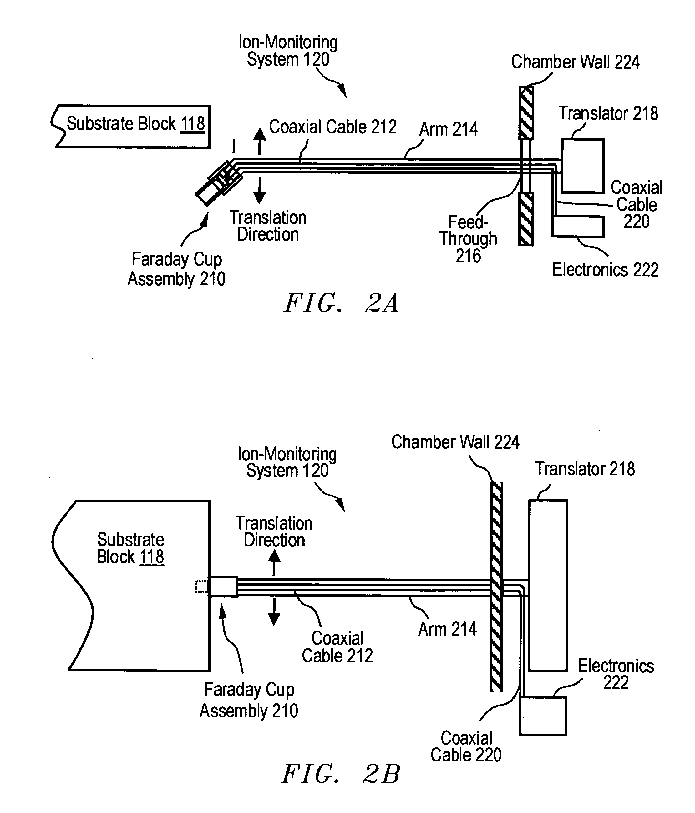
[0060] Another embodiment of the present invention replaces the ion-monitoring system 120 of the first embodiment with an array of multiple ion-monitoring instruments.

[0061]FIG. 4 shows an ion-monitoring array 600 according to another embodiment. The ion-monitoring array 600 includes multiple instantiations of the Faraday cup assembly 210 functionally connected to corresponding multiple instantiations of the shield cable 212, which in turn are functionally connected to the electronics 612 such that a signal line exists from each of the multiple instantiations of the shield cable 212 through the arm 214. The arm 214 passes through the feed-through 216 such that the arm 214 is free to move laterally and longitudinally within the feed-through 216 of the chamber wall 224 while maintaining a seal capable of withstanding pressures down to 10−7 Torr. The arm 214 is functionally connected to the translator 218 and a cable 610, which in turn is functionally connected to the electronics 612, ...

second embodiment

[0065]FIG. 5. illustrates a method 800 of using the ion-monitoring array 600 of the invention, including the following steps:

[0066] Step 810: Starting Process

[0067] In this step, the tape 112 translates through the IBAD system 100 and is subjected to a deposition process in which the tape 112 is exposed to a depositing species emitted from the e-beam evaporator 114 while undergoing simultaneous ion bombardment from the ion source 116.

[0068] Step 812: Positioning Array

[0069] In this step, the translator 218 translates the ion-monitoring array 600 along the deposition zone, which exists below the substrate block 118, such that the Faraday cup assemblies 210 encounter ions emitted from the ion source 116 at an angle of about 55 degrees from the normal of the tape 112.

[0070] Step 814: Collecting Ions

[0071] In this step, the ion-monitoring array 600 collects ion emissions from the ion source 116 and communicates the data to the controller 122.

[0072] Step 816: Ion Emission within Ra...


PUM

PropertyMeasurementUnit
Tcaaaaaaaaaa
acceptance angleaaaaaaaaaa

Abstract

A method of forming a superconductive device is provided, including providing a substrate having a dimension ratio of not less than about 102, depositing a buffer film to overlie the substrate by ion beam assisted deposition utilizing and ion beam, monitoring spatial ion beam density of the ion beam over a target area, and depositing a superconductor layer to overlie the buffer film. Monitoring may be carried out by utilizing an ion detector having an acceptance angle of not less than 10°.

Description

CROSS-REFERENCE TO RELATED APPLICATION(S) BACKGROUND [0001] 1. Field of the Invention [0002] The present invention is generally directed to superconductive articles, and more specifically methods for forming superconductive articles. [0003] 2. Description of the Related Art [0004] Superconductor materials have long been known and understood by the technical community. Low-temperature (low-Tc) superconductors exhibiting superconductive properties at temperatures requiring use of liquid helium (4.2 K), have been known since about 1911. However, it was not until somewhat recently that oxide-based high-temperature (high-Tc) superconductors have been discovered. Around 1986, a first high-temperature superconductor (HTS), having superconductive properties at a temperature above that of liquid nitrogen (77 K) was discovered, namely YBa2Cu3O7−x (YBCO), followed by development of additional materials over the past 15 years including Bi2Sr2Ca2Cu3O10+y (BSCCO), and others. The development of h...

Claims


Application Information

Patent Timeline
Patent Type & Authority Applications(United States)
IPC IPC(8): C23C14/00C23C14/08C23C14/46C23C14/54C23C14/58G01R19/00H01L39/24
CPCC23C14/081C23C14/46H01L39/2461C23C14/584G01R19/0061C23C14/54H10N60/0632
Inventor SELVAMANICKAM, VENKATXIONG, XUMING
Owner SUPERPOWER INC
Why Eureka
Try Eureka