Thin film transistor device and method of manufacturing the same

a technology of thin film transistor and manufacturing method, which is applied in the direction of identification means, instruments, crystal growth process, etc., can solve the problems of increasing production cost, difficult to apply such operating layer to the large and high-definition liquid crystal display panel, etc., and achieve the effect of reducing the number of masking steps and reducing the production cost of the thin film transistor devi

Inactive Publication Date: 2005-11-10
UNIFIED INNOVATIVE TECH
View PDF11 Cites 3 Cited by
  • Summary
  • Abstract
  • Description
  • Claims
  • Application Information

AI Technical Summary

Benefits of technology

[0022] It is an object of the present invention to provide a thin film transistor device capable of reducing the number of masking steps, and a method of manufacturing the same.
[0029] Accordingly, the number of masking steps can be reduced in contrast to the prior art, and thus the production cost of the thin film transistor device can be reduced.
[0033] In the present invention, the display electrode is formed in this manner. Therefore, the number of masking steps can be reduced in contrast to the prior art, and thus the production cost of the thin film transistor device can be reduced.
[0036] In the present invention, the display electrode is formed in this manner. Therefore, the number of masking steps can be reduced in contrast to the prior art, and thus the production cost of the thin film transistor device can be reduced.
[0042] In the present invention, in this manner, the display electrode and the gate electrode having the terrace structure are formed by one masking step. Therefore, the number of masking step can be reduced rather than the prior art and also the production cost of the thin film transistor device can be reduced.

Problems solved by technology

However, since the carrier mobility is small in the amorphous silicon, there exists such a drawback that it is hard to apply such operating layer to the large and high-definition liquid crystal display panel.
That is, the method in the prior art needs a number of masking steps, which cause the increase of the production cost.

Method used


Image

  • Thin film transistor device and method of manufacturing the same
  • Thin film transistor device and method of manufacturing the same
  • Thin film transistor device and method of manufacturing the same

Examples


first embodiment

[0056]FIG. 2 is a block diagram showing a configuration of a thin film transistor device (transmissive liquid crystal display panel) according to a first embodiment of the present invention. In the following example, the XGA (1024×768 pixel) mode liquid crystal display panel will be explained hereunder.

[0057] The liquid crystal display panel according to the present embodiment consists of a control circuit 101, a data driver 102, a gate driver 103, and a display portion 104. The signals such as display signals RGB (R (red) signal, G (green) signal, and B (blue) signal), a horizontal synchronizing signal Hsync, a vertical synchronizing signal Vsync, etc. are supplied to this liquid crystal display panel from the external devices (not shown) such as the computer, etc. Also, a high voltage VH (e.g., 18 V), a low voltage VL (e.g., 3.3 V or 5 V) and a ground potential Vgnd are supplied to the liquid crystal display panel from the power supplies (not shown).

[0058] In the display portion...

second embodiment

[0109]FIG. 19 is a circuit diagram showing a thin film transistor device according to a second embodiment of the present invention. The present embodiment shows an example in which the present invention is applied to an organic EL display panel.

[0110] A plurality of data bus lines 191 and power supply lines 192, which extend in the vertical direction, and a plurality of scanning bus lines 193, which extend in the horizontal direction, are formed on the glass substrate. Areas that are partitioned by the data bus lines 191, the power supply lines 192, and the scanning bus lines 193 are the pixel area respectively.

[0111] A switching TFT 194, a driving TFT 195, a capacitor 196, and an organic EL element (light emitting element) 197 are provided to each pixel area respectively.

[0112] A gate of the switching TFT 194 is connected to the scanning bus line 193, a source of the switching TFT 194 is connected to a gate of the driving TFT 195, and a drain of the switching TFT 194 is connecte...

third embodiment

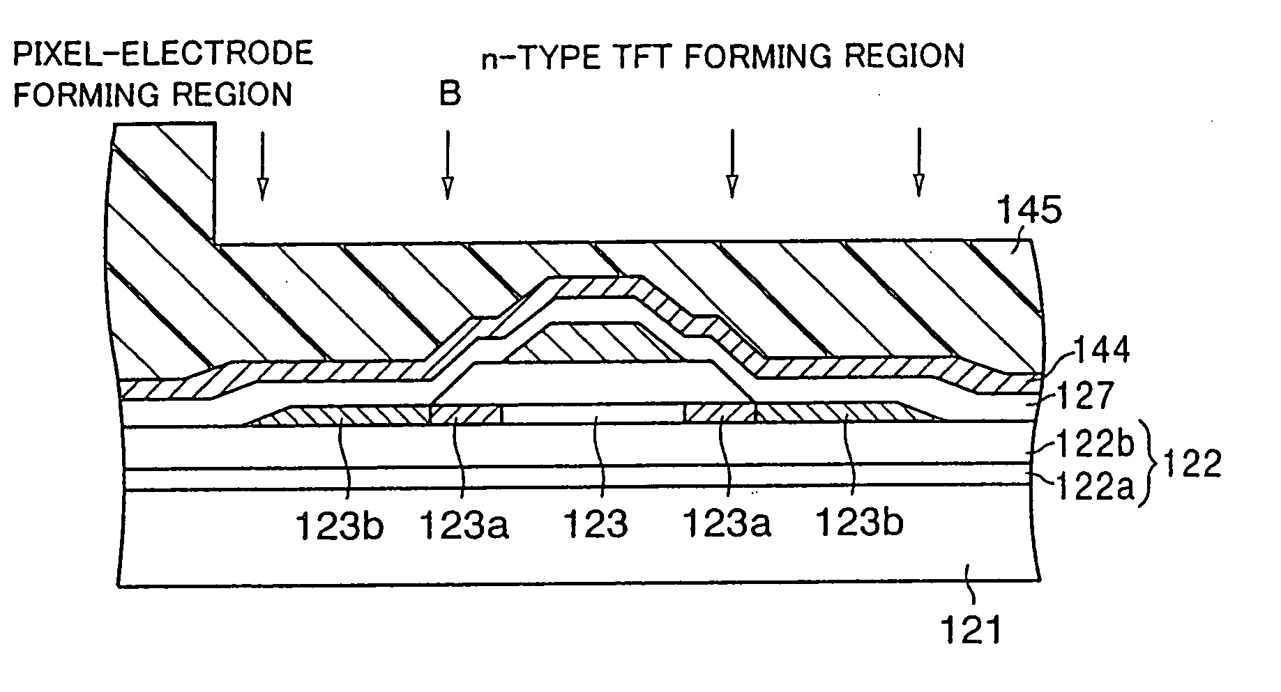
[0121]FIGS. 21A to 21M are sectional views showing a method of manufacturing a thin film transistor device (liquid crystal display panel) according to a third embodiment of the present invention in order of step. In these Figures, for convenience of explanation, the pixel TFT (n-type TFT) is illustrated on the left side and also the p-type TFT of the peripheral circuit is illustrated on the right side. Actually, the pixel TFTs are formed in the display region and the peripheral circuit is formed on the outside of the display region. Also, since the n-type TFTs of the peripheral circuit can be formed similarly to the pixel TFTs, illustration and explanation of them will be omitted herein.

[0122] First, as shown in FIG. 21A, a buffer layer 202 having a double-layered structure consisting of a SiN film 202a of 50 nm thickness and a SiO2 film 202b of 200 nm thickness is formed on a glass substrate (transparent insulating substrate) 201 by depositing sequentially SiN and SiO2 by virtue o...


PUM

PropertyMeasurementUnit
voltageaaaaaaaaaa
voltageaaaaaaaaaa
voltageaaaaaaaaaa

Abstract

A polysilicon film is formed in a predetermined region on a glass substrate, and then a gate insulating film and a gate electrode, whose width is narrower than the gate insulating film, are formed thereon. Then, an interlayer insulating film and an ITO film are formed on an overall surface. Then, n-type source / drain regions having an LDD structure are formed by implanting the n-type impurity into the polysilicon film. Then, an n-type TFT forming region and a pixel-electrode forming region are covered with a resist film, and then p-type source / drain regions are formed by implanting the p-type impurity into the polysilicon film in a p-type TFT forming region. Then, the resist film is left only in the pixel-electrode forming region and the resist film is removed from other regions. A pixel electrode is formed by etching the ITO film while using the remaining resist film as a mask.

Description

CROSS-REFERENCE TO RELATED APPLICATIONS [0001] This application is based upon and claims priority of Japanese Patent Application No. 2001-401483, filed in Dec. 28, 2001, the contents being incorporated herein by reference. BACKGROUND OF THE INVENTION [0002] 1. Field of the Invention [0003] The present invention relates to a thin film transistor device having thin film transistors (abbreviated as “TFTs” hereinafter) used in a liquid crystal display panel, an organic EL display panel, etc. and a method of manufacturing the same. [0004] 2. Description of the Prior Art [0005] The liquid crystal display panel has such merits that such panel is thin and light in weight and the consumption power is small because such panel can be driven by the low voltage, and is widely employed in various electronic devices such as PDA (Personal Digital Assistant), the finder of the video camera, and others. In particular, since the active-matrix liquid crystal display panel, in which the switching elemen...

Claims


Application Information

Patent Timeline
Patent Type & Authority Applications(United States)
IPC IPC(8): C30B1/00G02F1/1368G09F9/30H01L21/00H01L21/20H01L21/336H01L21/36H01L21/77H01L21/84H01L27/01H01L27/12H01L29/04H01L29/10H01L29/15H01L29/423H01L29/49H01L29/786H01L31/036H01L31/0376H01L31/20
CPCH01L27/1214H01L27/3248H01L29/42384H01L29/4908H01L2029/7863H01L29/78621H01L2227/323H01L27/1288H01L29/66757H10K59/123H10K59/1201H01L29/786
Inventor HOTTA, KAZUSHIGEYAEGASHI, HIROYUKIWATANABE, TAKUYAWADA, TAMOTSU
Owner UNIFIED INNOVATIVE TECH
Why Eureka
Try Eureka