Method for manufacturing resistively switching memory devices

a technology of resistively switching memory and memory cell, which is applied in the direction of digital storage, semiconductor devices, instruments, etc., can solve the problems of cbram memory cell not being able to meet the requirements of cbram memory cell, amorphicity of probes may be lost, and the electrical resistance between electrodes may vary relatively strongly

Inactive Publication Date: 2005-11-10
ADESTO TECH
View PDF7 Cites 71 Cited by
  • Summary
  • Abstract
  • Description
  • Claims
  • Application Information

AI Technical Summary

Benefits of technology

[0026] The present invention provides a method that enables a reproducible conditioning during the manufacturing of a CBRAM memory cell, and a system with such a memory device. The present invention includes, in particular, providing a method by which it is possible to control the diffusion of the ions in the chalcogenide material of the CBRAM memory cell and to thus optimize the concentration profile between the doped and the undoped phase of the chalcogenide matrix.

Problems solved by technology

One difficulty with this switching process in a CBRAM memory cell consists in that the electric resistance between the electrodes may vary relatively strongly with a particular state of the cell (“conductive” or “non-conductive”).
A further difficulty consists in that the CBRAM memory cell does not comprise any reproducible switching properties in the “unconditioned” state.
A drawback of the thermal method consists in that the amorphicity of the probe may be lost since a nanocrystallization with subsequent grain growth occurs which substantially changes the nanostructure or microstructure, respectively, of the probe.
The ion movability of the metal doping substance is, however, as a rule by magnitudes smaller in crystalline materials, which may involve a significant degradation of the memory cell properties.
A drawback of the photo diffusion process consists i.a. in that the doping profile is very steep due to the photo-stimulated doping process since the movability of the ions is distinctly higher in the metal-rich phase.
The electric forming pulse is, however, incompatible with some semiconductor manufacturing processes of mass products since an electrical conditioning does not guarantee sufficient reproducibility.
A drawback of the implantation process consists in that extremely high doses of metal have to be implanted, which requires a very high implantation performance and / or a very long duration of the implantation process.
A further difficulty results from the fact that the implanted doping courses are formed very flatly since otherwise an undesired mixing or, in the case of too deep implantation profile courses, an electric short-circuit will be caused.

Method used


Image

  • Method for manufacturing resistively switching memory devices
  • Method for manufacturing resistively switching memory devices
  • Method for manufacturing resistively switching memory devices

Examples


Embodiment Construction

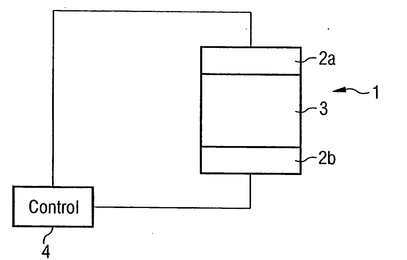
[0051]FIG. 1 shows schematically and by way of example the structure of a resistively switching memory cell 1 and a central control device 5 connected thereto.

[0052] On an appropriate memory device or memory chip, respectively, a plurality of further memory cells that are of a structure similar or identical to the memory cell 1 illustrated in FIG. 1 may be arranged, e.g. in an appropriate memory cell field positioned side by side in a plurality of rows or columns. In the following, the basic functioning of a resistively switching memory cell is illustrated by way of example.

[0053] The memory cells 1 may be any kind of resistively switching memory cells, e.g. Phase Change Memory Cells or CBRAM memory cells (CB=Conductive Bridging). Controlled by a central control device 5 provided on the memory device, specific writing or deleting processes may be performed in the memory cells 1 of the memory device.

[0054] As results from FIG. 1, each of the above-mentioned memory cells 1 comprise...


PUM


Abstract

The present invention relates to a reproducible conditioning during the manufacturing of a resistively switching CBRAM memory cell comprising a first electrode and a second electrode with an active material positioned therebetween. The active material is adapted to be placed in a more or less electroconductive state by means of electrochemical switching processes. A CBRAM memory cell manufactured pursuant to the method according to the invention has, due to the improved conditioning, more reliable and more distinctly evaluable electrical switching properties. Moreover, no more forming step is necessary with the method according to the present invention.

Description

CLAIM FOR PRIORITY [0001] This application claims priority to German Application No. 10 2004 020 297.4 filed Apr. 26, 2004, which is incorporated herein, in its entirety, by reference. TECHNICAL FIELD OF THE INVENTION [0002] The invention relates to a method for manufacturing a resistively switching memory cell, and to a memory device, in particular a resistively switching memory device, and a system including such a memory device. BACKGROUND OF THE INVENTION [0003] In the case of conventional memory devices, in particular conventional semiconductor memory devices, one differentiates between so-called functional memory devices (e.g. PLAs, PALs, etc.) and so-called table memory devices, e.g. ROM devices (ROM=Read Only Memory)—in particular PROMs, EPROMs, EEPROMs, flash memories, etc.—, and RAM devices (RAM=Random Access Memory or read-write memory), e.g. DRAMs (Dynamic Random Access Memory or dynamic read-write-memory) and SRAMs (Static Random Access Memory or static read-write-memor...

Claims


Application Information

Patent Timeline
Patent Type & Authority Applications(United States)
IPC IPC(8): G11C13/02H01L21/336H01L21/8239H01L27/24H01L45/00
CPCG11C13/0011H01L45/085H01L45/1675H01L45/141H01L45/1658H01L45/1233H10N70/245H10N70/882H10N70/826H10N70/046H10N70/063
Inventor UFERT, KLAUS DIETERPINNOW, CAY-UWE
Owner ADESTO TECH
Why Eureka
Try Eureka