
Multiple selectable function integrated circuit module

a multi-functional, integrated circuit technology, applied in the direction of semiconductor/solid-state device testing/measurement, semiconductor/dram wafer details, instruments, etc., can solve the problem of increasing the difficulty in planning the production of dram wafers, complicating the semiconductor processing, and adding an extra step in the processing of functional integrated circuit dies. fuse destruction, reduce the variety of integrated circuit components, reduce the effect of the required inventory of integrated circuit components

Inactive Publication Date: 2005-11-10
QUALCOMM INC
View PDF14 Cites 7 Cited by
  • Summary
  • Abstract
  • Description
  • Claims
  • Application Information

AI Technical Summary

Benefits of technology

This approach reduces the inventory of integrated circuit components and simplifies the manufacturing process by allowing the selection of functions during packaging, thereby minimizing the number of assembly types required and maintaining a single common design for multiple selectable functions.

Problems solved by technology

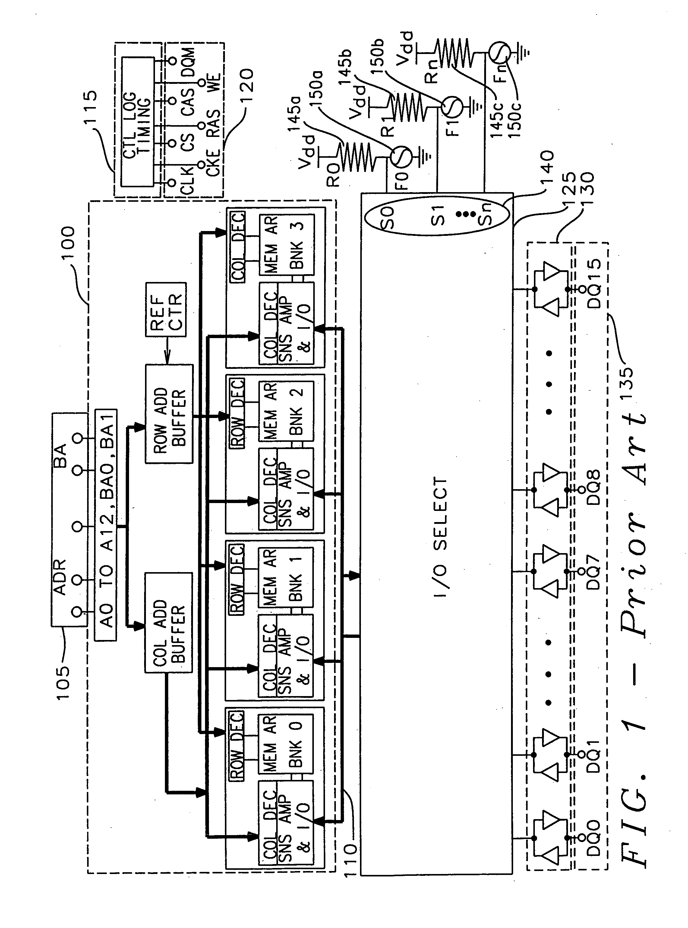
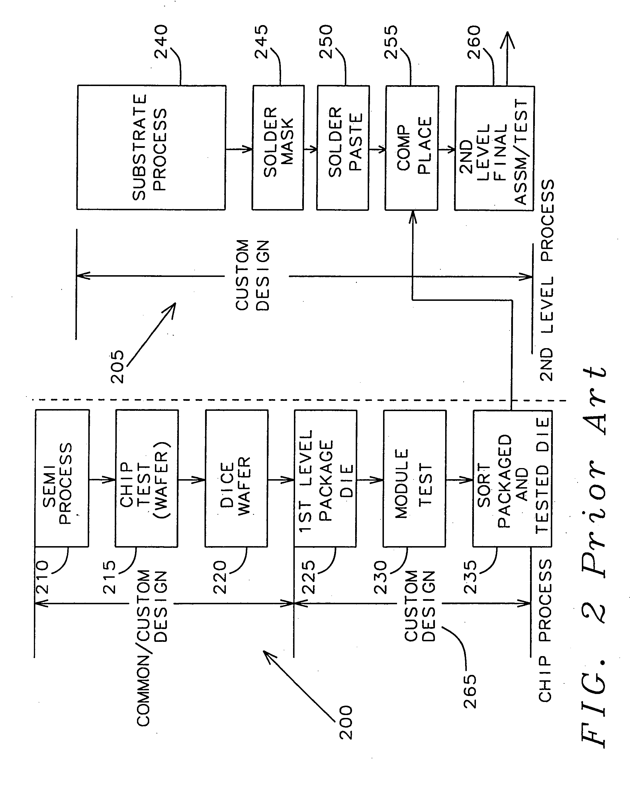
The fused configuration selection forces the maintenance of inventory of the DRAM die for each desired configuration increasing the difficulty in planning of production of DRAM wafers.
This complicates the semiconductor processing in that extra masking steps are required for mask programming of desired functions of the functional integrated circuit die.
Additionally, fuse destruction adds an extra step in the processing of the functional integrated circuit die.

Method used


Image

  • Multiple selectable function integrated circuit module
  • Multiple selectable function integrated circuit module
  • Multiple selectable function integrated circuit module

Examples


first embodiment

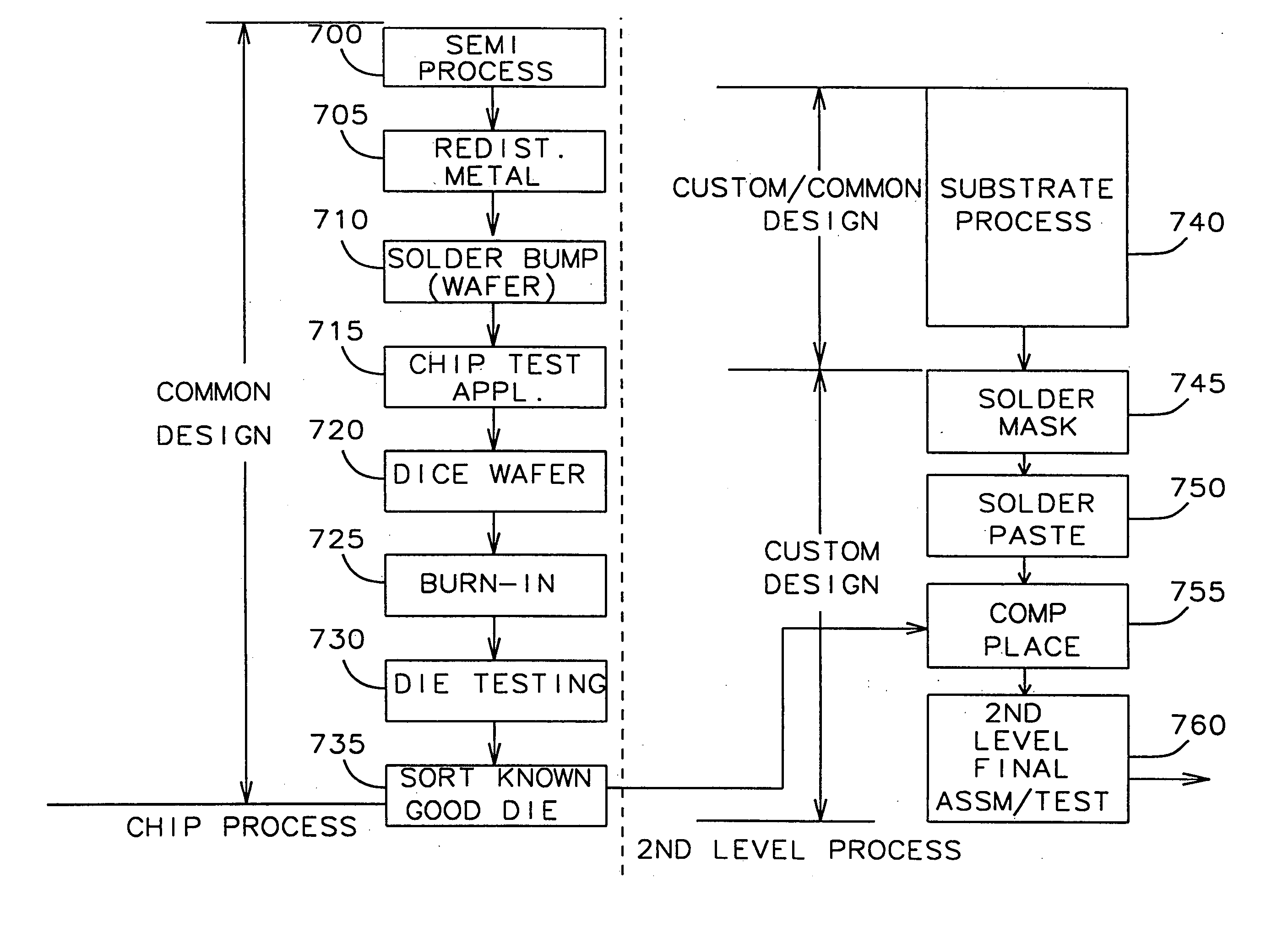
[0080] For discussion of a method for assembling and selecting desired options of a multiple, selectable function integrated circuit module of the first embodiment, refer to FIG. 7. A multiple selectable function integrated circuit die is formed 700 on a semiconductor wafer by formation and interconnection of electronic circuits on the semiconductor wafer employing known semiconductor processes. Redistribution metal is fabricated 705 on the surface of the semiconductor wafer forming the connections of the common internal functions and the selectable internal functions of the multiple selectable function integrated circuit die to input / output pads on the surface of the semiconductor wafer. The solder bumps are then formed and reflowed to form 710 the solder ball on the surface of the semiconductor wafer. The individual multiple selectable function integrated circuit dies are then tested 715 and the functional multiple selectable function integrated circuit dies are identified. The se...

second embodiment

[0092] Refer now to FIG. 9 for a discussion of the present invention. The integrated circuit 300 is designed and fabricated as described in FIG. 3. However instead of being place directly on a module that is effectively the second level or system package, the integrated circuit 300 is mounted and secured to the first level or module package 900. The input / output pads 314, 322, 330, 338, 342, 350, and 358 are respectively connected to the interconnection pads 918, 958, 932, 954, 946, 966, and 974 of the first level package 900 respectively by the connections 916, 960, 931, 953, 948, 968, and 976. The connections 916, 960, 931, 953, 948, 968, and 976 are permanently established when the integrated circuit 300 is mounted and secured to the first level package 900. Thus, the first level package 900, in effect, becomes a space transform to transform the maximum spacings allowed of the integrated circuit 300 to the minimum spacings allowed by the second level package 302.

[0093] The interc...


PUM


Abstract

An integrated circuit module has a common function known good integrated circuit die with selectable functions. The selectable functions are selected during packaging of the known good integrated circuit die. The known good integrated circuit die is mounted to a second level substrate. The second level substrate has wiring connections to the input / output pads of the known good integrated circuit die that select desired input functions and output functions. Further, the wiring connections on the second level substrate provide signal paths to transfer signals to the desired input function and signals from the desired output function, and signals to and from the common functions. Also, the wiring connections form connections between the input / output pads and external circuitry. To select the desired input functions and the desired output functions, appropriate logic states are applied to input / output pads connected to a function selector to configure a functional operation of the integrated circuit module. The second level module substrate has connector pins to provide physical and electrical connections between the external circuitry and the wiring connections on the second level substrate.

Description

RELATED PATENT APPLICATIONS [0001] This application is related to the U.S. patent application Ser. No. 09 / 258,911, filing date Mar. 1, 1999, now U.S. Pat. No. 6,180426 B1, issued Jan. 30, 2001. [0002] This application is a Continuation-in-Part of U.S. patent application Ser. No. 09 / 246,303, filing date Feb. 8, 1999.BACKGROUND OF THE INVENTION FIELD OF THE INVENTION [0003] 1. Field of the Invention [0004] This invention is related to integrated circuits. More particularly, this invention relates to multiple function integrated circuits such as Dynamic Random Access Memories (DRAM) having function selection through wiring connections on a second level substrate onto which an integrated circuit is mounted. [0005] 2. Background of the Related Art [0006] The structure of a DRAM is well known in the art. Usually a DRAM chip is configured to be organized as a ×1 (by 1), ×4 (by 4), ×8 (by 8), or ×16 (by 16) package by selective destruction of fuses internal to the DRAM chip and by selective...

Claims


Application Information

Patent Timeline
Patent Type & Authority Applications(United States)
IPC IPC(8): G06F3/00G06F7/38H01L21/66H01L23/495H01L23/538H01L29/40
CPCH01L22/20H01L22/22H01L2224/49171H01L2924/014H01L2224/48237H01L23/5382
Inventor LIN, MOU-SHIUNG
Owner QUALCOMM INC
Learn More