Methods of fabricating structures for characterizing tip shape of scanning probe microscope probes and structures fabricated thereby

a technology of scanning probe and microscope probe, which is applied in the field of structure fabrication for characterizing the tip shape of scanning probe microscope probe and the structure fabricated thereby, can solve the problems of introducing additional distortions into the image data, the feature size approaches the microscope resolution limit, and the inability to directly image the small probe tip with sufficient accuracy

Inactive Publication Date: 2005-11-17
BRUKER NANO INC
View PDF24 Cites 23 Cited by
  • Summary
  • Abstract
  • Description
  • Claims
  • Application Information

AI Technical Summary

Problems solved by technology

Moreover, the shape of the probe tip may change during scanning due to wear or the probe tip may become contaminated by foreign debris, thus introducing additional distortions into the image data.
As the dimensions of probe tips shrink for imaging shrinking IC features, the feature sizes approach the microscope resolution limit.
As a result, small probe tips are impossible to directly image with sufficient accuracy to provide correction factors for AFM image data.
Such conventional characterizers are plagued by numerous deficiencies.
One problem is that the pillar must be narrow to provide the best resolution for tip width measurements (which are made by scanning the probe tip over the pillar) and, concurrently, the overhang distance of the edge should be wider than the boot width of the probe tip.
Satisfying both requirements would require an extremely thin pillar susceptible to fracture when struck by the probe tip during characterization.
Another problem is observed when the probe tip and the characterizer pillar are aligned with a nonparallel relationship.
This problem arises if, for example, the characterizer is mismounted in the AFM, the probe tip is mismounted in the AFM cantilever holder, or the characterizer pillars fail to meet specification and results in an inability to accurately characterize the boot shape.
Specifically, in these situations, the probe tip may contact the sidewall of the pillar rather than the edge, which prevents accurate measurement of the boot shape on one side of the probe tip.
Yet another problem with conventional characterizers may occur if the AFM has a clamping function that prevents profiling below a given depth of a sample, typically a depth exceeding the length of the probe tip.
The clamping function may interfere with the calibration process using conventional characterizers.
Conventional characterizers are limited in the extent to which the shape of a probe tip may be characterized.
Conventional characterizers lack the ability to accurately characterize concavity on the bottom surface of the boot if the probe tip width is equal to, or less than, the width of the edges.
Another limitation observed with conventional characterizers is that most only include parallel structures, which means that shape measurements may only be made in one direction as the probe tip is translated across the characterizer.
As a result, the characterizer must be reoriented for characterizing additional portions of the probe tip, which cannot be dismounted from the AFM during characterization.

Method used


Image

  • Methods of fabricating structures for characterizing tip shape of scanning probe microscope probes and structures fabricated thereby
  • Methods of fabricating structures for characterizing tip shape of scanning probe microscope probes and structures fabricated thereby
  • Methods of fabricating structures for characterizing tip shape of scanning probe microscope probes and structures fabricated thereby

Examples


Embodiment Construction

[0021] Although the invention will be described next in connection with certain embodiments, the invention is not limited to practice in any one specific type of atomic force microscope (AFM). Exemplary AFM's in which the principles of the invention can be practiced are commercially available, for example, from Veeco Metrology Group (Santa Barbara, Calif.). The description of the invention is intended to cover all alternatives, modifications, and equivalent arrangements as may be included within the spirit and scope of the invention as defined by the appended claims.

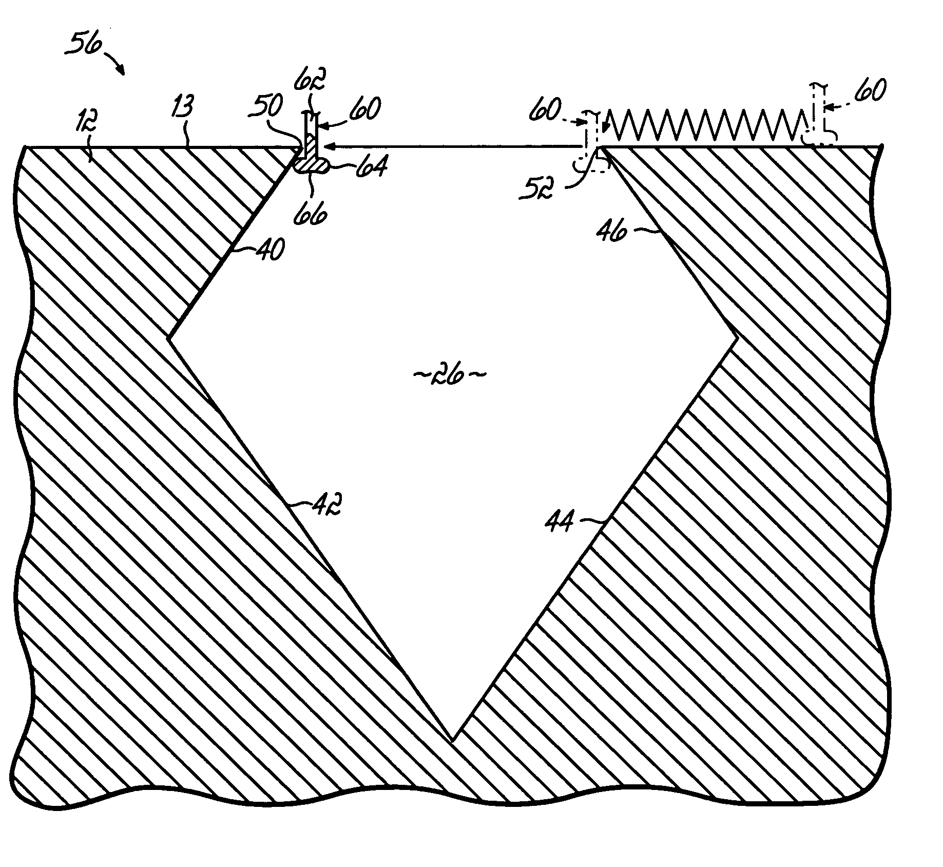
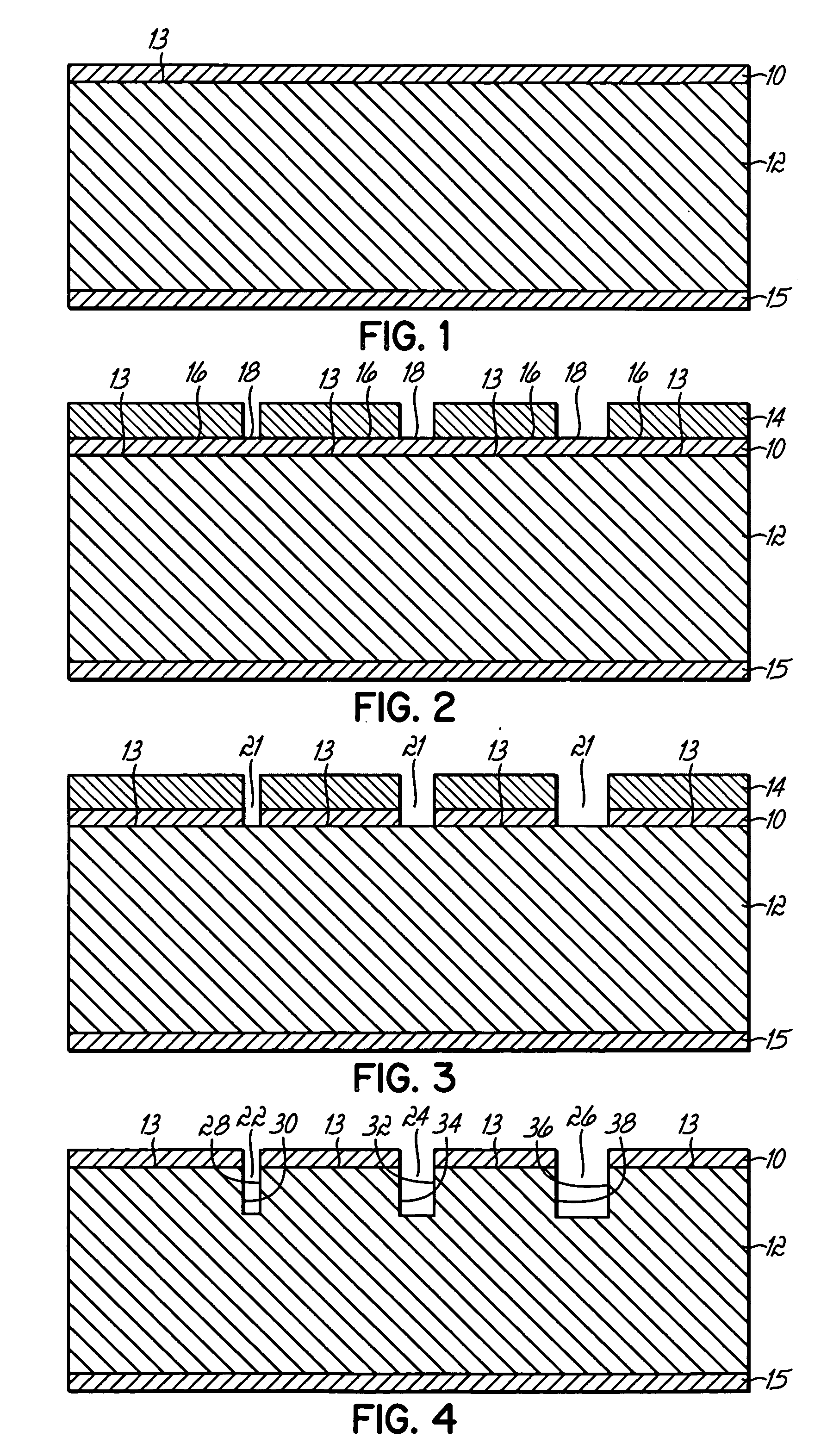
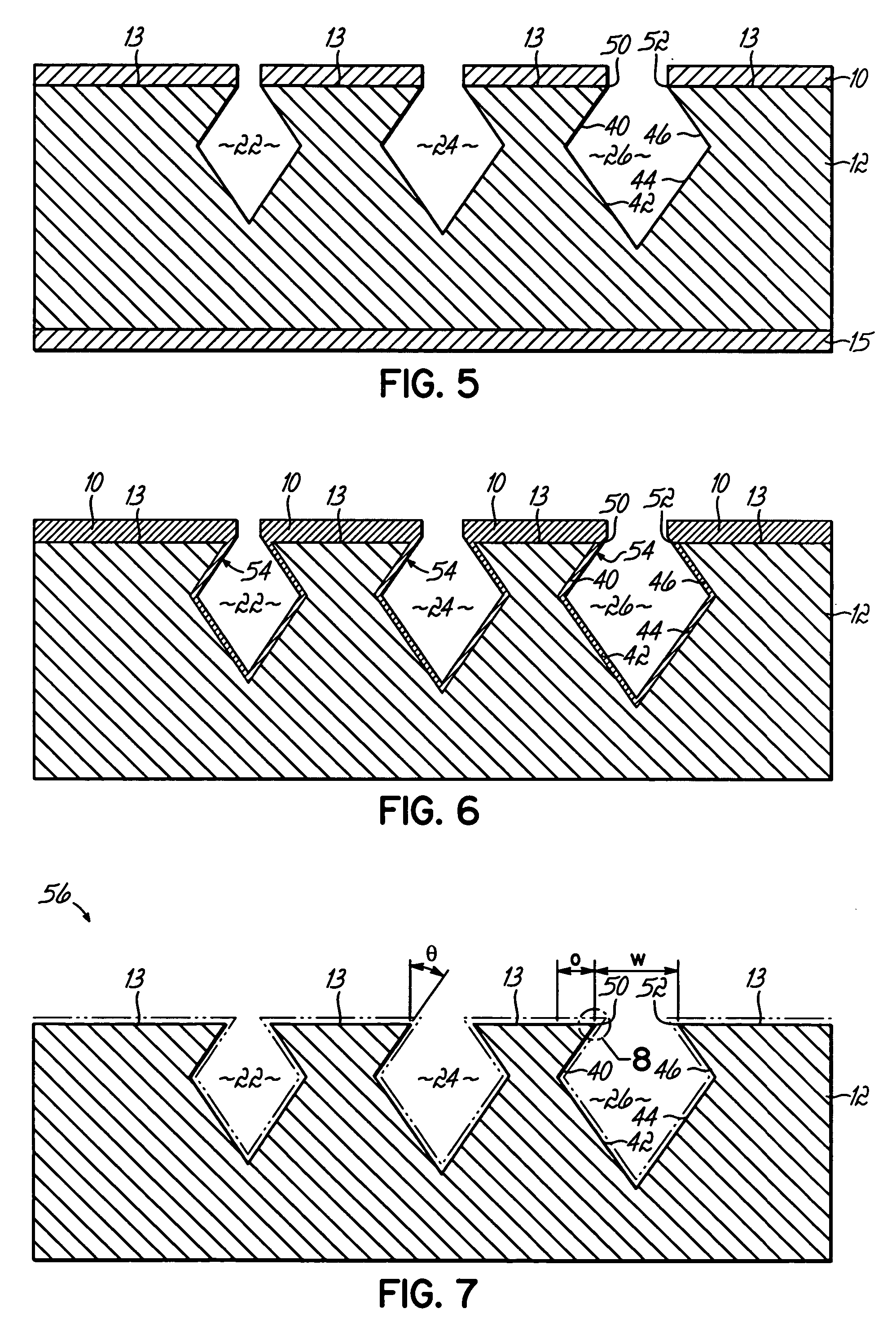
[0022] With reference to FIG. 1, a hard mask 10 is formed as a uniformly thick surface layer on a single crystal substrate 12, which is characterized by a substantially-planar upper surface 13. A layer 15 of the hard mask material may also be formed on a backside of the substrate 12. In a specific embodiment of the invention, substrate 12 is a (100) silicon wafer characterized by a resistivity of one-tenth (0.1) ohm-cm ...


PUM


Abstract

A characterizer for determining the shape of a probe tip for an atomic force microscope and methods of fabricating and using the characterizer. The characterizer includes a micromachined crystalline structure with opposed edges separated by a width suitable for characterizing a dimension of the probe tip. At least one of the opposed edges overhangs an undercut region of the micromachined crystalline structure by an overhang distance that is greater than one third of the width. The probe tip is scanned across the edges of the characterizer for shape determination. The characterizer is formed by serially deep reactive ion etching and anisotropic etching (100) single crystal silicon. The opposed edges may be oxidation sharpened for use in profiling a bottom surface of the probe tip.

Description

FIELD OF THE INVENTION [0001] The invention relates to probe microscopy and, more particularly, to methods of fabricating structures for characterizing the tip shape of probes used in a scanning probe microscope and structures formed by such methods. BACKGROUND OF THE INVENTION [0002] Atomic force microscopes (AFM's) were developed, among other reasons, to meet a demand for accurately measuring critical dimensions (CDs) during integrated circuit (IC) fabrication. Critical dimensions constitute the width of a line or space, such as the width of a patterned line, the distance between two lines or devices, or the size of a contact, on a substrate identified as crucial for proper operation of the device being fabricated. Critical dimensions are measured on some or all substrates following any photolithography or etching process in which the dimensions are critical. Due to their high spatial resolution, AFM's are well suited for measuring critical dimensions during IC fabrication. [0003]...

Claims


Application Information

Patent Timeline
Patent Type & Authority Applications(United States)
IPC IPC(8): G01B5/28G01Q10/00G01Q40/00G01Q40/02
CPCG01Q40/02B82Y35/00
Inventor CHAND, AMIOKULAN, NIHAT
Owner BRUKER NANO INC
Why Eureka
Try Eureka