Use of scanning probe microscope for defect detection and repair

a scanning probe and microscope technology, applied in semiconductor/solid-state device testing/measurement, instruments, nuclear engineering, etc., can solve the problems of processing silicon wafer defects, less progress in repairing defects, and defects in processed silicon wafers. achieve the effect of precise correction of defects

Inactive Publication Date: 2005-04-26
GLOBALFOUNDRIES INC
View PDF17 Cites 40 Cited by
  • Summary
  • Abstract
  • Description
  • Claims
  • Application Information

AI Technical Summary

Benefits of technology

[0011]The present invention provides a system and method for detecting and repairing defects in semiconductor devices. According to the invention, defects are located using a scanning probe microscope, such as an atomic force microscope or a scanning tunneling microscope, and repaired at locations determined by the scanning probe microscope. The microscope itself, and in particular the detection tip, may be employed to remove the defects. For example, the tip may be used to machine away the defect, to apply an electric field to oxidize the defect, and / or to heat the defect causing it to burn or vaporize. By combining precise defect location capabilities of a scanning probe microscope with defect removal, the invention permits very precise correction of defects such as excess material and foreign particles on semiconductor substrates.

Problems solved by technology

Defects in the mask or the patterned resist may result in defects in the processed wafer.
In spite of advances in lithographic procedures, processed silicon wafers sometimes have defects, such as excess material or particulate contaminants.
While there has been significant progress in detecting defects, less progress has been made in repairing defects.
There is an unsatisfied need for a system and method of repairing defects in semiconductor devices with small features.

Method used


Image

  • Use of scanning probe microscope for defect detection and repair
  • Use of scanning probe microscope for defect detection and repair
  • Use of scanning probe microscope for defect detection and repair

Examples


Embodiment Construction

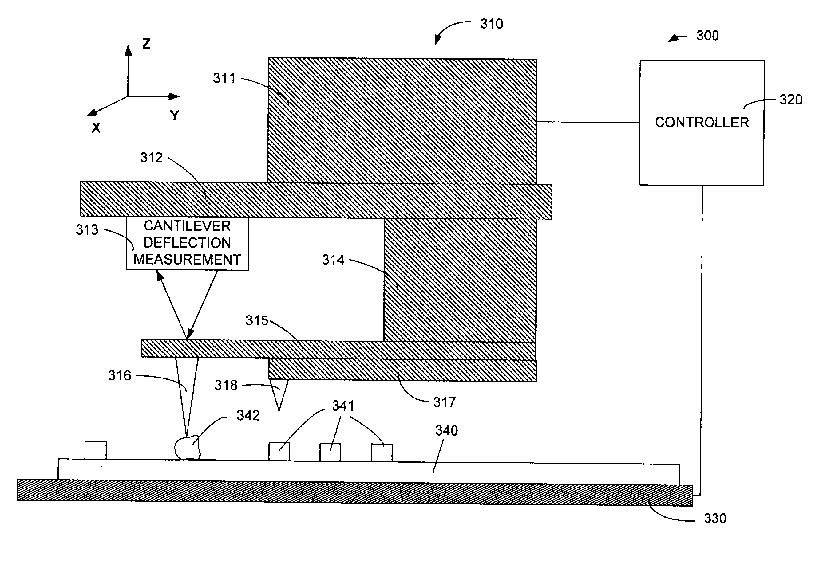
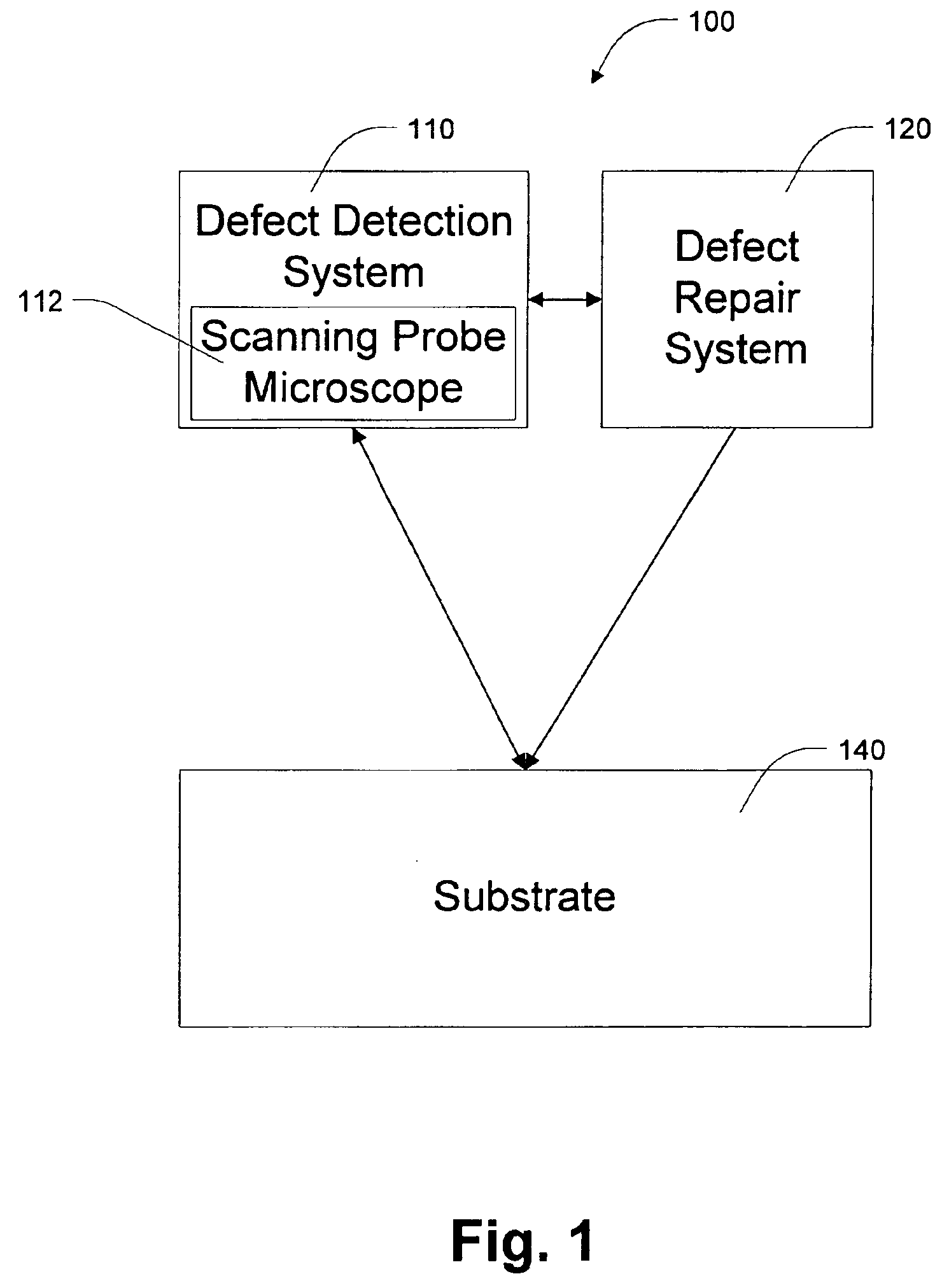
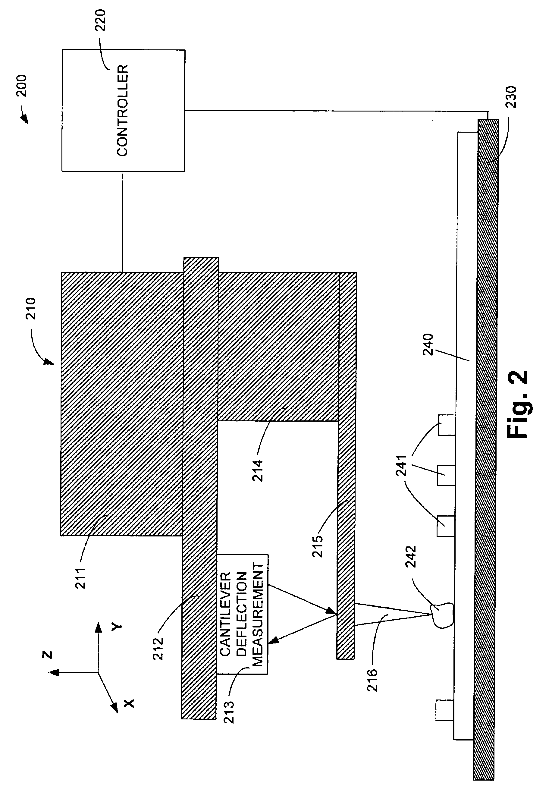
[0021]FIG. 1 is a high level schematic of a system 100 according to one aspect of the present invention. System 100 includes defect detection system 110 and defect repair system 120, which may be combined in one apparatus. Defect detection system 10 includes scanning probe microscope 112. Defect repair system 120 repairs defects in substrate 140 at locations determined by defect detection system 10. Defect detection system 10 may transfer a defect map to defect repair system 120 or, where the systems are combined, may repair defects using scanning probe microscope 112. By combining defect repair with a scanning probe microscope's sensitive defect location ability, system 100 is able to carry out very precise repairs.

[0022]While the invention can be applied to any type of substrate, it is applied in particular to semiconductor substrates. A semiconductor substrate includes a semiconducting material, such as silicon. In addition to a semiconducting material, the substrate may include ...


PUM

PropertyMeasurementUnit
normal forceaaaaaaaaaa

Abstract

The present invention provides a system and method for detecting and repairing defects in semiconductor devices. According to the invention, defects are located using a scanning probe microscope, such as an atomic force microscope or a scanning tunneling microscope, and repaired at locations determined by the scanning probe microscope. The microscope itself, and in particular the detection tip, may be employed to remove the defects. For example, the tip may be used to machine away the defect, to apply an electric field to oxidize the defect, and/or to heat the defect causing it to burn or vaporize. By combining precise defect location capabilities of a scanning probe microscope with defect removal, the invention permits very precise correction of defects such as excess material and foreign particles on semiconductor substrates.

Description

CROSS REFERENCE TO RELATED APPLICATIONS[0001]This application claims the benefit of U.S. Provisional Patent Application Ser. No. 60 / 242,834, filed Oct. 24, 2000, entitled USED OF SCANNING PROBE MICROSCOPE FOR DEFECT DETECTION AND REPAIR.TECHNICAL FIELD[0002]The present invention generally relates to semiconductor processing, and in particular to a method of detecting and repairing defects in a semiconductor or other type of workpiece.BACKGROUND OF THE INVENTION[0003]In the semiconductor industry, there is a continuing trend toward higher device densities. To achieve these high densities there have been, and continue to be, efforts toward scaling down the device dimensions on semiconductor wafers. In order to accomplish higher device density, smaller and smaller features sizes are required. These may include the width and spacing of interconnecting lines, spacing and diameter of contact holes, and surface geometry of corners and edges of various features.[0004]High resolution lithogr...

Claims


Application Information

Patent Timeline
Patent Type & Authority Patents(United States)
IPC IPC(8): G11C13/00G21K7/00G11B9/00G01Q60/00G01Q70/10H01L21/66
CPCH01L22/20G01Q80/00Y10S977/855Y10S977/874H01L2924/0002H01L2924/00
Inventor YEDUR, SANJAY K.SINGH, BHANWARCHOO, BRYAN K.
Owner GLOBALFOUNDRIES INC
Why Eureka
Try Eureka