Display filter, display device including the display filter, and method of manufacturing the display filter

a display device and filter technology, applied in the direction of identification means, instruments, diffusion transfer processes, etc., can solve the problems of phosphor surface reflection, adversely affecting humans, increase in electromagnetic radiation, etc., to enhance the em shielding property, enhance the contrast of the display device, and facilitate the manufacture of such a display filter

Inactive Publication Date: 2005-11-17
SAMSUNG ELECTRONICS CO LTD +1
View PDF6 Cites 36 Cited by
  • Summary
  • Abstract
  • Description
  • Claims
  • Application Information

AI Technical Summary

Benefits of technology

[0012] It is a feature of an embodiment of the present invention to provide a display filter that can enhance contrast of a display device in a bright room.
[0013] It is another feature of an embodiment of the present invention to provide a display filter that can enhance an EM shielding property.
[0014] It is yet another feature of an embodiment of the present invention to provide a method for readily manufacturing such a display filter.
[0016] At least one of the above and other features and advantages of the present invention may be realized by providing a display filter for use with a plurality of microlenses in a display system, the display filter including an external light and electromagnetic (EM) shielding portion including a photosensitive transparent resin layer and an external light and EM-shielding pattern, the photosensitive transparent resin layer having a photocatalyst, the external light and EM-shielding pattern formed on regions of the photosensitive transparent resin layer to prevent external light from entering the display system and to prevent EM waves generated in the display system from exiting the display system, the regions corresponding to boundaries between the plurality of microlenses.
[0021] At least one of the above and other features and advantages of the present invention may be realized by providing a method of manufacturing a display filter for use with a plurality of microlenses in a display system, the method including forming a photosensitive transparent resin layer having a photocatalyst, and forming an external light and electromagnetic EM-shielding pattern on regions of the photosensitive transparent resin layer to prevent external light from entering the display system and to prevent EM waves generated in the display system from exiting the display system, the regions corresponding to boundaries between the plurality of microlenses.

Problems solved by technology

Despite the above advantages, PDPs have several problems associated with driving characteristics, including an increase in electromagnetic (EM) radiation, near-infrared (NIR) emission, phosphor surface reflection, and an obscured color purity due to orange light emitted from helium (He) or xenon (Xe) that is used as a sealing gas.
The EM radiation generated by PDPs may adversely affect humans and cause electronic devices, e.g., wireless telephones or remote controls, to malfunction.
However, conventional PDP filters cannot prevent external light from entering a panel assembly, leading to reduction in contrast in bright viewing conditions.
This external light may interfere with light emitted from a discharge cell in the panel assembly, thereby lowering contrast, ultimately degrading the image displayed on the PDPs.

Method used


Image

  • Display filter, display device including the display filter, and method of manufacturing the display filter
  • Display filter, display device including the display filter, and method of manufacturing the display filter
  • Display filter, display device including the display filter, and method of manufacturing the display filter

Examples


first embodiment

[0040]FIG. 2 illustrates a cross-sectional view of a PDP filter according to the present invention.

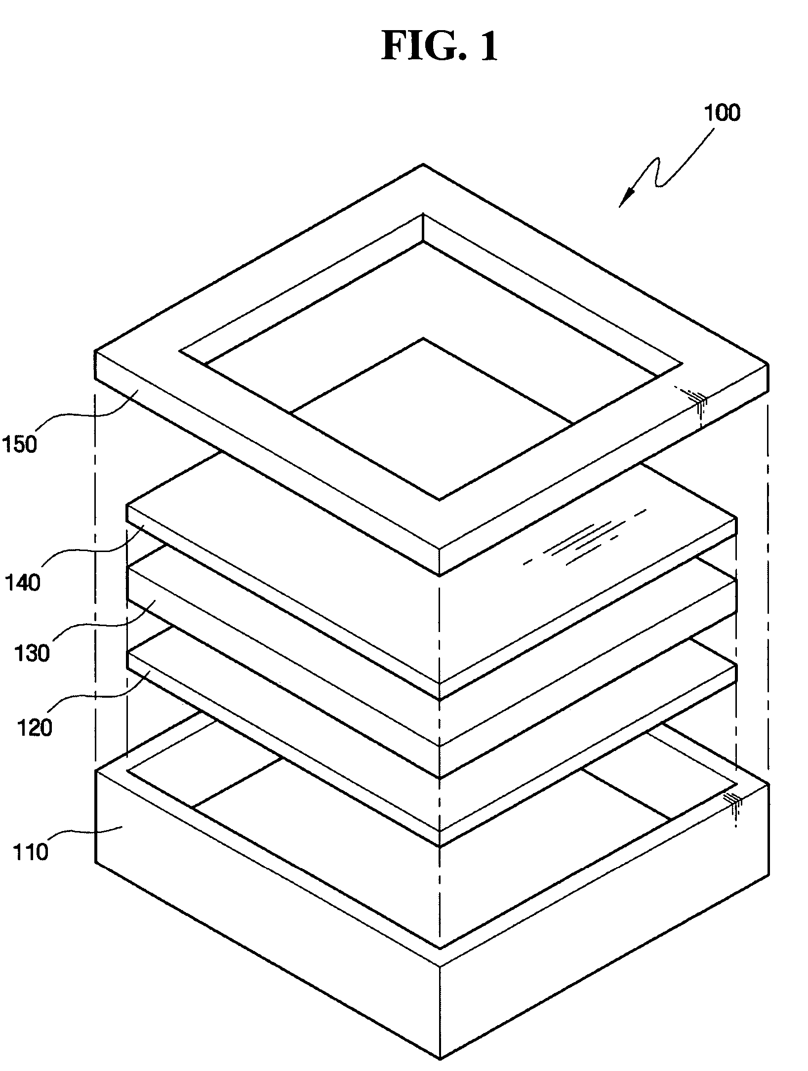
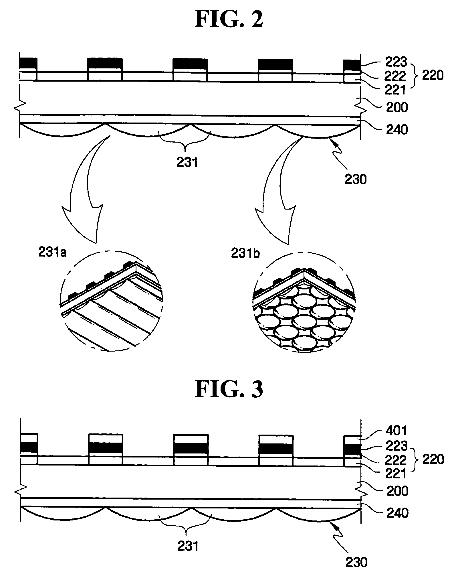
[0041] Referring to FIG. 2, the PDP filter of the first embodiment includes a filter base 200 and an external light and EM-shielding portion 220 formed on a surface of the filter base 200. A light-focusing portion 230 may be formed on a surface of the filter base 200 opposite the external light and EM-shielding portion 220. A support 240 for the light-focusing portion 230 may also be included.

[0042] The light-focusing portion 230 faces the panel assembly 130, shown in FIG. 1, and focuses light generated from the panel assembly. The light-focusing portion 230 may include of a plurality of microlenses 231.

[0043] The external light and EM-shielding portion 220 prevents both external light from entering the panel assembly and specific EM waves from exiting the panel assembly. The external light and EM-shielding portion 220 may formed in a stripe pattern or a mesh pattern. The external li...

fourth embodiment

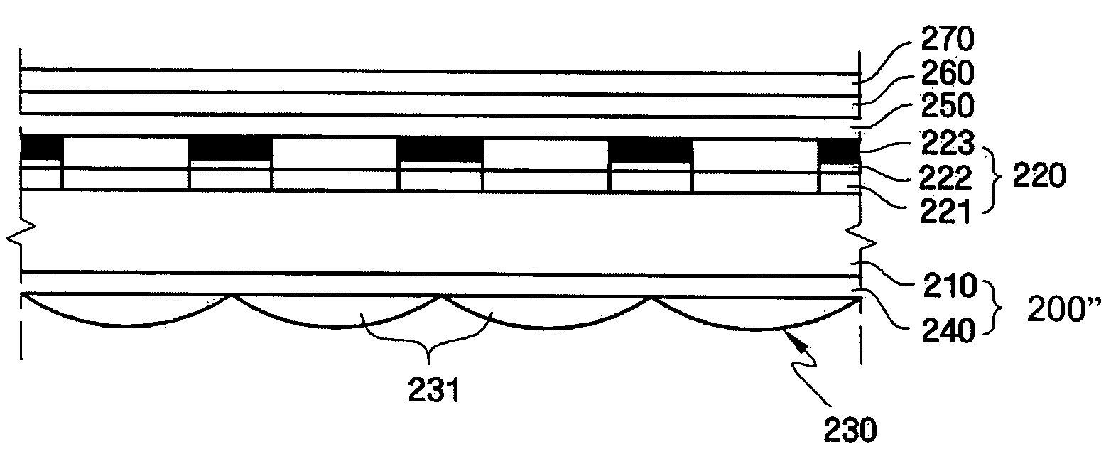
[0061]FIG. 5 illustrates a cross-sectional view of a PDP filter according to the present invention. Referring to FIG. 5, the filter base 200″ is just the transparent substrate 210. The external light and EM-shielding portion 220 is on the transparent substrate 210, and the orange light-shielding layer 250, the NIR-shielding layer 260, and the AR layer 270 are sequentially stacked on external light and EM-shielding portion 220.

[0062] The stacking sequence of the orange light-shielding layer 250, the NIR-shielding layer 260, and the AR layer 270 may be modified, but it is preferable that the AR layer 270 be in the topmost position. Additional orange light-shielding, NIR-shielding, and / or AR layers may also be included.

[0063] Material used for the transparent substrate 210 is not particularly limited, as long as provided that it has a visible light transmittance of about 80% or more, good thermal resistance, and sufficient strength. For example, the transparent substrate 210 may be ma...

second embodiment

[0072] Hereinafter, a method for forming the external light and EM-shielding portion in the PDP filter according to the present invention shown in FIG. 3 is discussed in detail. FIGS. 6A through 6F illustrate cross-sectional views of stages in an embodiment of a method for forming the external light and EM-shielding portion.

[0073] Referring to FIG. 6A, the photosensitive transparent resin layer 221 is formed on an entire surface of the filter base 200.

[0074] The photosensitive transparent resin layer 221 may be a polymer material containing a photocatalyst. Preferably, the polymer material used for the photosensitive transparent resin layer 221 is a vinyl alcohol resin, an acrylic resin, or a cellulosic resin. For example, the vinyl alcohol resin may be an ethylene-vinyl alcohol copolymer or a vinyl acetate-vinyl alcohol copolymer. The acrylic resin may be polyacrylamide, polymethylol acrylamide, or a copolymer thereof. The cellulosic resin may be nitrocellulose, acetylpropyl cellu...


PUM


Abstract

A display filter for use with a plurality of microlenses in a display system includes an external light and electromagnetic (EM)-shielding portion having a photosensitive transparent resin layer with a photocatalyst, and an external light and EM-shielding pattern formed on regions of the photosensitive transparent resin layer to prevent external light from entering the display system and to prevent EM waves generated in the display device from exiting the display device, the regions corresponding to boundaries between the plurality of microlenses.

Description

BACKGROUND OF THE INVENTION [0001] 1. Field of the Invention [0002] The present invention relates to a display filter, a display device including the display filter, and a method of manufacturing the display filter. More particularly, the present invention relates to a display filter that enhances contrast of a display device viewed in a bright room, a display device including the display filter, and a method of manufacturing the display filter. [0003] 2. Description of the Related Art [0004] As modern society becomes more information-oriented, the technology of photoelectronic devices and apparatuses is advancing, and these devices are becoming widespread. In particular, image display devices are in widespread use in devices such as TV screens and PC monitors. Thinly built wide screens have become mainstream display devices. [0005] In particular, a plasma display panel (PDP) is gaining popularity as a next-generation display device to replace a cathode ray tube (CRT) because it is ...

Claims


Application Information

Patent Timeline
Patent Type & Authority Applications(United States)
IPC IPC(8): G02B5/22G09F9/00H01J11/12H01J11/44H01J17/49H05K9/00
CPCH01J11/12H01J2211/446H01J11/44H01J9/205H01J2211/444H01J2217/49292H01J2329/869
Inventor PARK, DAE-CHULCHOI, YONG-WONJUNG, SANG-CHEOLCHOI, WANG-KYU
Owner SAMSUNG ELECTRONICS CO LTD
Why Eureka
Try Eureka