Liquid crystal display device

US20050253980A1Inactive Publication Date: 2005-11-17HITACHI DISPLAYS

Image

  • Liquid crystal display device
  • Liquid crystal display device
  • Liquid crystal display device

Examples


embodiment 1

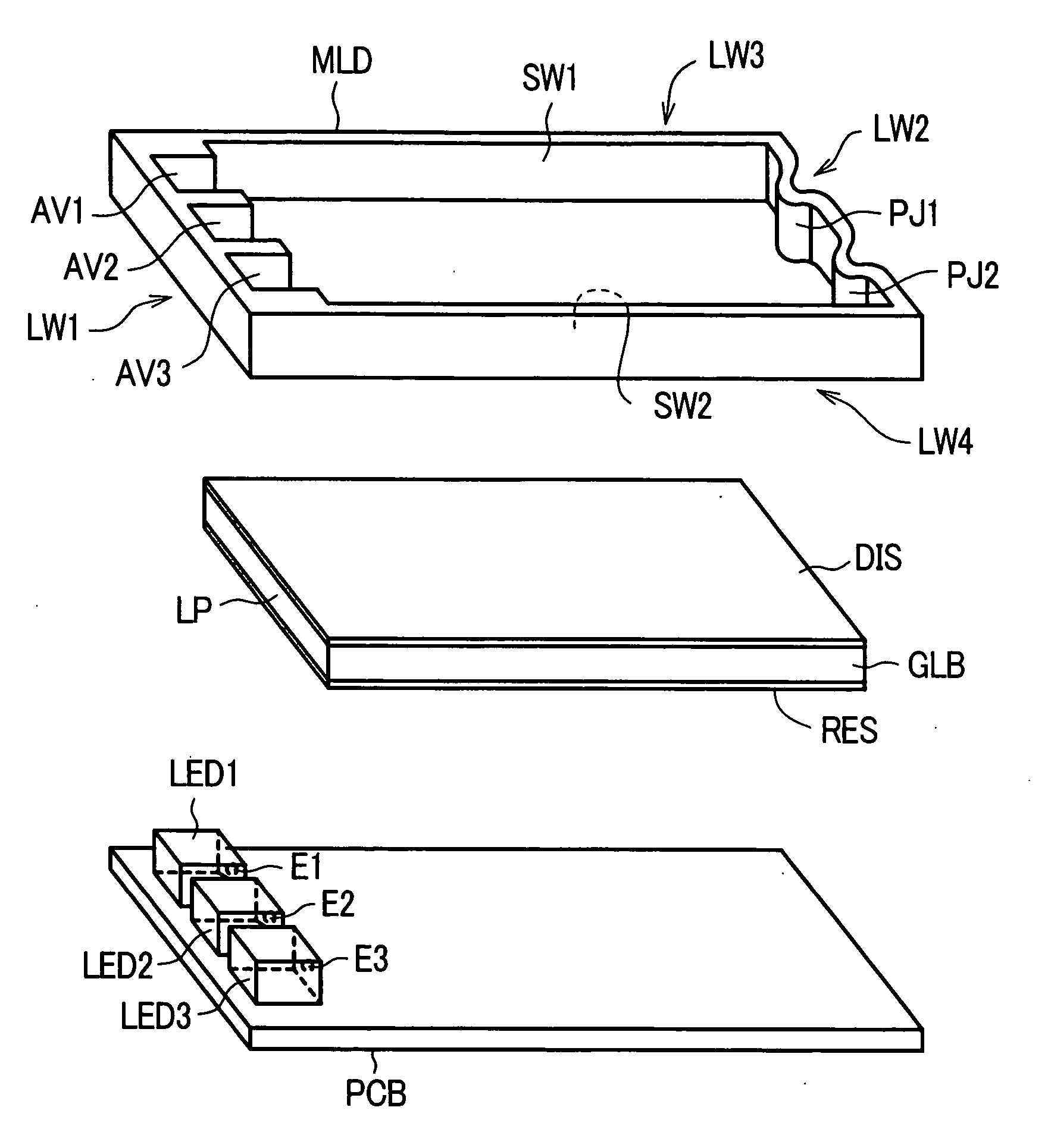
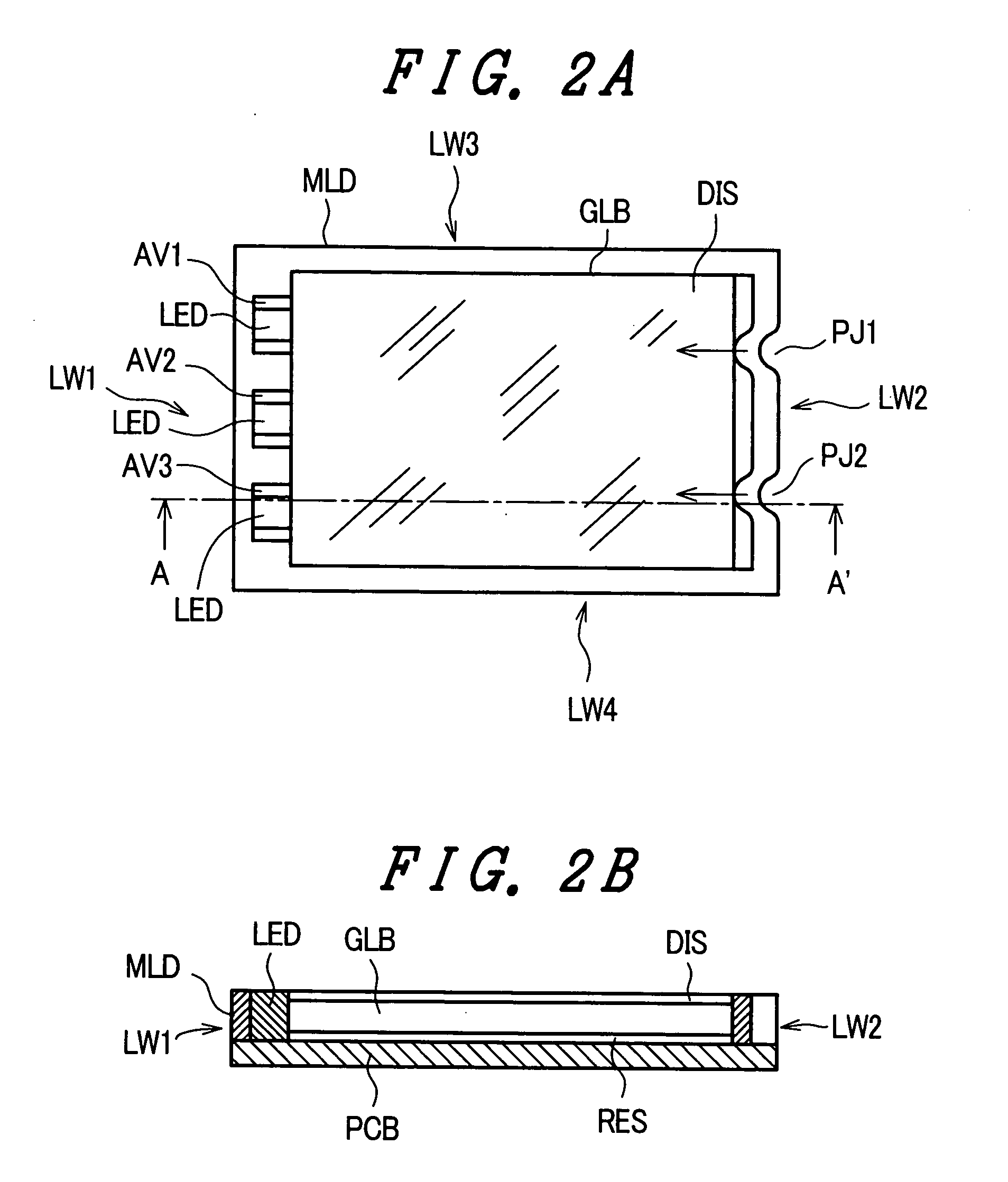
[0031]FIG. 1 is a developed perspective view showing the constitution of an essential part excluding a liquid crystal display panel, a housing case and the like for explaining an embodiment 1 of a liquid crystal display device according to the invention. In FIG. 1, a mold case MLD is an approximately rectangular frame-like body. The mold case MLD is, as a whole, made of a resin material having resiliency. In an inner wall of a first side LW1 of the mold case MLD, accommodating portions AV1, AV2, AV3 for accommodating light emitting diodes LED1, LED2, LED3 which constitute light emitting elements are formed. Further, curved projections J1, J2 which project inwardly are formed on a second side LW2 which is a side opposite to the first side LW1 of the mold case MLD.

[0032] A third side LW3 and a fourth side LW4 which are arranged close to the first side LW1 and the second side LW2 have inner walls SW1, SW2 which are arranged in parallel to each other. Reference symbol GLB indicates a l...


PUM

PropertyMeasurementUnit
depthaaaaaaaaaa
depthaaaaaaaaaa
radiusaaaaaaaaaa

Abstract

A liquid crystal display device includes a plurality of light emitting diodes mounted on a side wall of a light guide plate so as to irradiate light inside of the light guide plate. On a light reflection surface of the light guide plate, a plurality of light reflection patterns having concentric grooves about the light emitting diodes in the direction equal to the advancing direction of respective main light beams of the light emitting diodes are formed in a state that the plurality of light reflection patterns are divided into a first light reflection pattern region and a second light reflection pattern region respectively corresponding to the light emitting diodes. Between the first light reflection pattern region and a second light reflection pattern region, a light reflection pattern intersecting region where end portions of the light reflection patterns intersect each other is defined.

Description

CROSS-REFERENCE TO RELATED APPLICATIONS [0001] The disclosure of Japanese Patent Application No. 2004-113311 filed on Apr. 7, 2004 including the specification, drawings and abstract is incorporated herein by reference in its entirety. BACKGROUND OF THE INVENTION [0002] The present invention relates to a liquid crystal display device, and more particularly to a liquid crystal display device having a light guide plate which diffuses a light-source light of a solid light emitting element such as a light emitting diode or the like as a light source in a developed manner on a back surface of a liquid crystal display panel in a planer shape. [0003] Recently, with respect to a miniaturized portable digital assistant such as a mobile phone, a portable information terminal or the like, a liquid crystal display device which is small-sized and exhibits the low power consumption has been popularly used as a display device. As this type of liquid crystal display device, a liquid crystal display ...

Claims


Application Information

Patent Timeline
17 Nov 2005
Publication
US20050253980A1
IPC
F21V8/00; F21Y101/02; G02F1/133; G02F1/1333; G02F1/1335; G02F1/13357; G09F9/35
CPC
G02B6/0038; G02B6/0068; G02F1/133615; G02B6/0091; G02F1/133603; G02B6/0088
Inventors
SAITO, KEN; SHIMAMO, SHIGEO