Nitride semiconductor substrate and manufacturing method thereof

a technology of nitride semiconductor and substrate, which is applied in the direction of polycrystalline material growth, crystal growth process, chemically reactive gas, etc., can solve the problems of difficult growth of gan film epitaxially on the base substrate, difficulty in nitride semiconductor, and use of high-cost base substrate and additional growth apparatus, so as to achieve high quality and absorb or reduce stress

Inactive Publication Date: 2008-06-19
LG SILTRON
View PDF3 Cites 15 Cited by
  • Summary
  • Abstract
  • Description
  • Claims
  • Application Information

AI Technical Summary

Benefits of technology

[0026]As such, the present invention forms the trenches on the lower surface of the base substrate, and in particular, the present invention forms the trenches such that pitches of the trenches get smaller or the widths or depths of the trenches get larger from the central portion of the base substrate towards the peripheral portion, thereby sufficiently absorbing or reducing stresses applied larger from the central portion of the base substrate towards the peripheral portion. Therefore, the present invention can obtain a high quality nitride semiconductor substrate free of warpage or cracks in spite of use of a silicon base substrate that is known as hard to form a nitride semiconductor film thereon.

Problems solved by technology

However, the base substrate and the GaN film have different lattice constants and thermal expansion coefficients, which makes it difficult to grow epitaxially the GaN film on the base substrate.
This difficulty occurs to a nitride semiconductor including AlN, InN, GaInN, AlGaN and GaAlInN in the same way as GaN.
However, disadvantageously this method uses a high cost base substrate and an additional growth apparatus to form the buffer layer.
Thus, there is limitation in application to a laser diode or a light-emitting diode.
However, it requires much time to separate the sapphire base substrate and a separation yield is low.
However, it is not easy to grow the GaN film on the silicon base substrate so far, and the silicon base substrate is often etched during GaN film growth.
Further, although the GaN film is grown on the silicon substrate, warpage or cracks may occur to the base substrate due to differences in thermal expansion coefficient and lattice constant.
However, this patent uses the sapphire substrate as a base substrate for growing GaN, and thus requires a considerable time to separate the sapphire base substrate and has low separation yield.

Method used


Image

  • Nitride semiconductor substrate and manufacturing method thereof
  • Nitride semiconductor substrate and manufacturing method thereof
  • Nitride semiconductor substrate and manufacturing method thereof

Examples


Embodiment Construction

[0033]Hereinafter, preferred embodiments of the present invention will be described in detail with reference to the accompanying drawings. Prior to the description, it should be understood that the terms used in the specification and the appended claims should not be construed as limited to general and dictionary meanings, but interpreted based on the meanings and concepts corresponding to technical aspects of the present invention on the basis of the principle that the inventor is allowed to define terms appropriately for the best explanation. In the case that the following description shows a layer exists on another layer, this may be interpreted that the layer may exist directly on another layer or a third layer may be interposed therebetween.

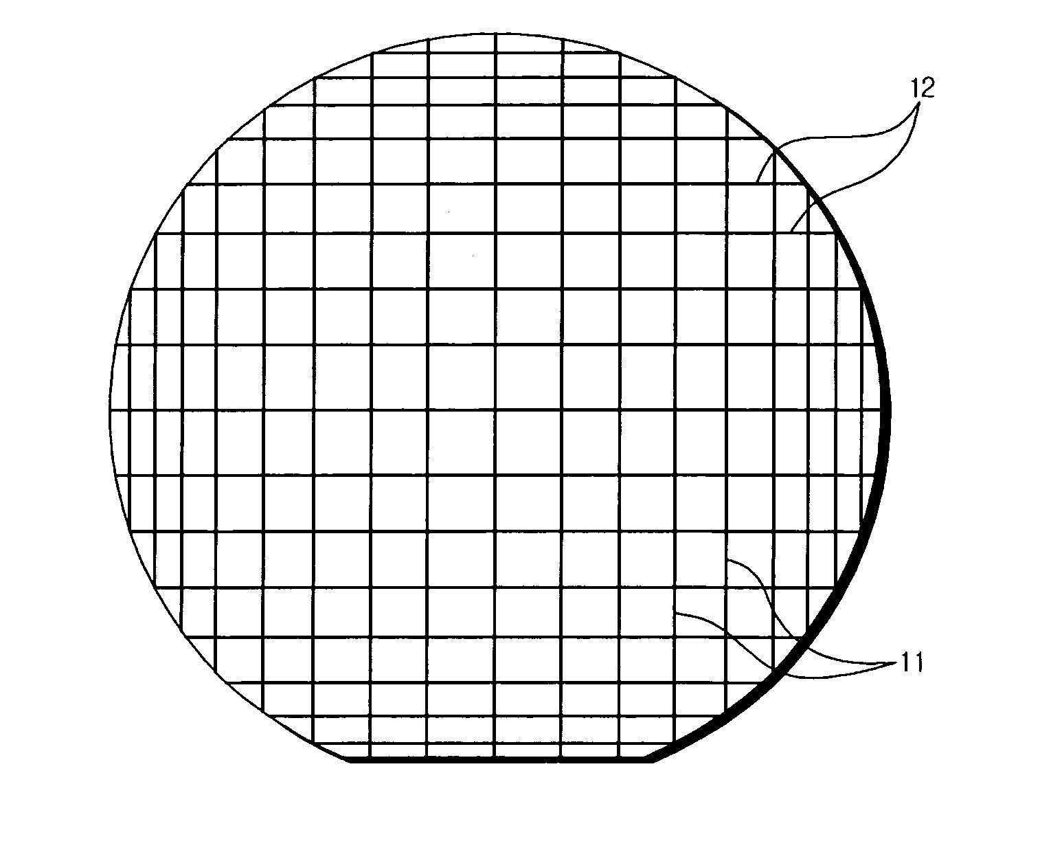
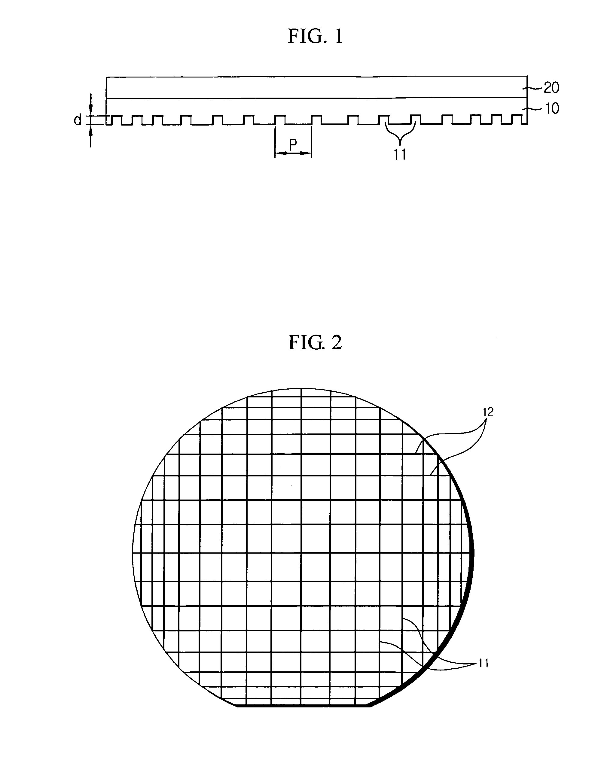
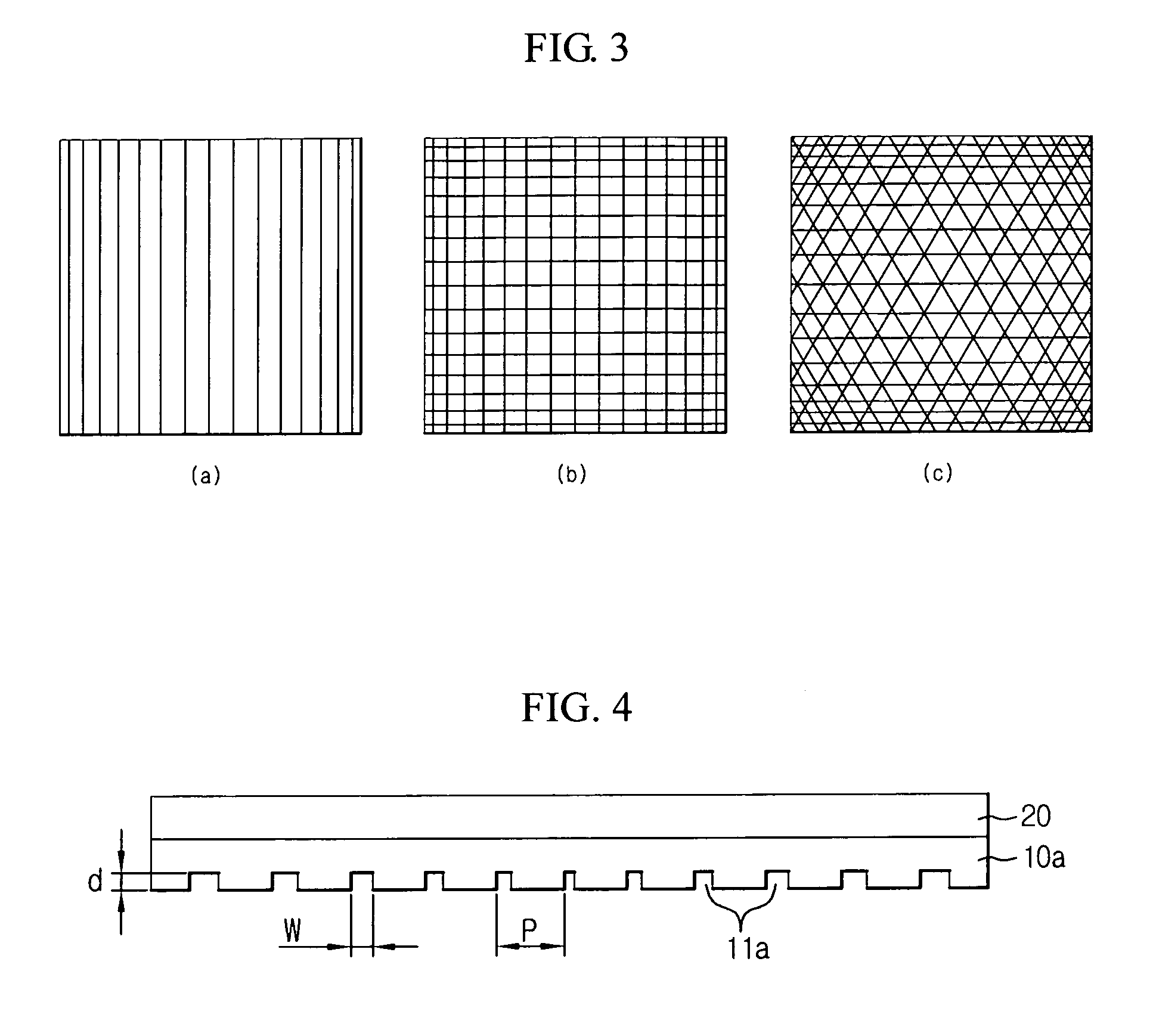
[0034]FIG. 1 is a cross-sectional view illustrating a gallium nitride (GaN) substrate manufactured according to an embodiment of the present invention. FIG. 2 is a bottom view illustrating the GaN substrate of FIG. 1. Referring to FIGS. 1 an...


PUM

PropertyMeasurementUnit
bandgap energyaaaaaaaaaa
widthsaaaaaaaaaa
thicknessaaaaaaaaaa

Abstract

The present invention relates to a nitride semiconductor substrate such as gallium nitride substrate and a method for manufacturing the same. The present invention forms a plurality of trenches on a lower surface of a base substrate that are configured to absorb or reduce stresses applied larger when growing a nitride semiconductor film on the base substrate from a central portion of the base substrate towards a peripheral portion. That is, the present invention forms the trenches on the lower surface of the base substrate such that pitches get smaller or widths or depths get larger from the central portion of the base substrate towards the peripheral portion.

Description

BACKGROUND OF THE INVENTION[0001]1. Field of the Invention[0002]The present invention relates to a nitride semiconductor substrate obtained by growing a nitride semiconductor film such as gallium nitride (GaN) film on a base substrate, and to a method for manufacturing the same.[0003]2. Description of the Related Art[0004]GaN is a nitride semiconductor having Wurzite structure, and has a direct transition bandgap of 3.4 eV corresponding to the blue wavelength range of visible rays at room temperature, forms a solid solution with InN and AlN to control a bandgap energy, and exhibits a characteristic of a direct transition semiconductor over the entire composition range of the solid solution. Thus, GaN is widely used as a material for a light emitting device, in particular a blue light emitting device.[0005]Generally, a GaN film is formed on a base substrate made of sapphire (Al2O3), silicon carbide (SiC) or silicon (Si) by MOCVD (Metal Organic Chemical Vapor Deposition) or HVPE (Hydr...

Claims


Application Information

Patent Timeline
Patent Type & Authority Applications(United States)
IPC IPC(8): H01L29/267H01L21/205C23C16/01C23C16/34C30B25/18C30B29/38
CPCH01L21/0237H01L21/02381H01L21/02658H01L21/0254H01L21/02428H01L21/20
Inventor KIM, DOO-SOOLEE, HO-JUNKIM, YONG-JINLEE, DONG-KUN
Owner LG SILTRON
Why Eureka
Try Eureka